Method for manufacturing a non-volatile memory device

Inactive Publication Date: 2005-04-28
SK HYNIX INC
View PDF4 Cites 16 Cited by
  • Summary
  • Abstract
  • Description
  • Claims
  • Application Information

AI Technical Summary

Benefits of technology

[0012] According to the method for manufacturing a non-volatile memory device according to the present invention, it is possible to obtain the capacitance by forming a trench in a cell region, forming a floating gate in a concave shap

Problems solved by technology

However, when increasing the surface area of the floating gate, it is difficult to increase the integration degree of a flash memory device.
Thus, it is hard to increase the capacitance by increasing the area of the floating gate.
Particularly, as the height of the floating gate in a SoC product storing an EEPROM cell becomes larger, the height of the control gate becomes lar

Method used


Image

  • Method for manufacturing a non-volatile memory device
  • Method for manufacturing a non-volatile memory device
  • Method for manufacturing a non-volatile memory device

Examples


Example

[0015] Hereinafter, a preferred embodiment of the present invention will be described in more detail referring to the drawings. In addition, the following embodiment is for illustration only, not intended to limit the scope of the invention.

[0016]FIGS. 1a to 1j are sectional views sequentially showing a method for manufacturing a non-volatile memory device according to the present invention.

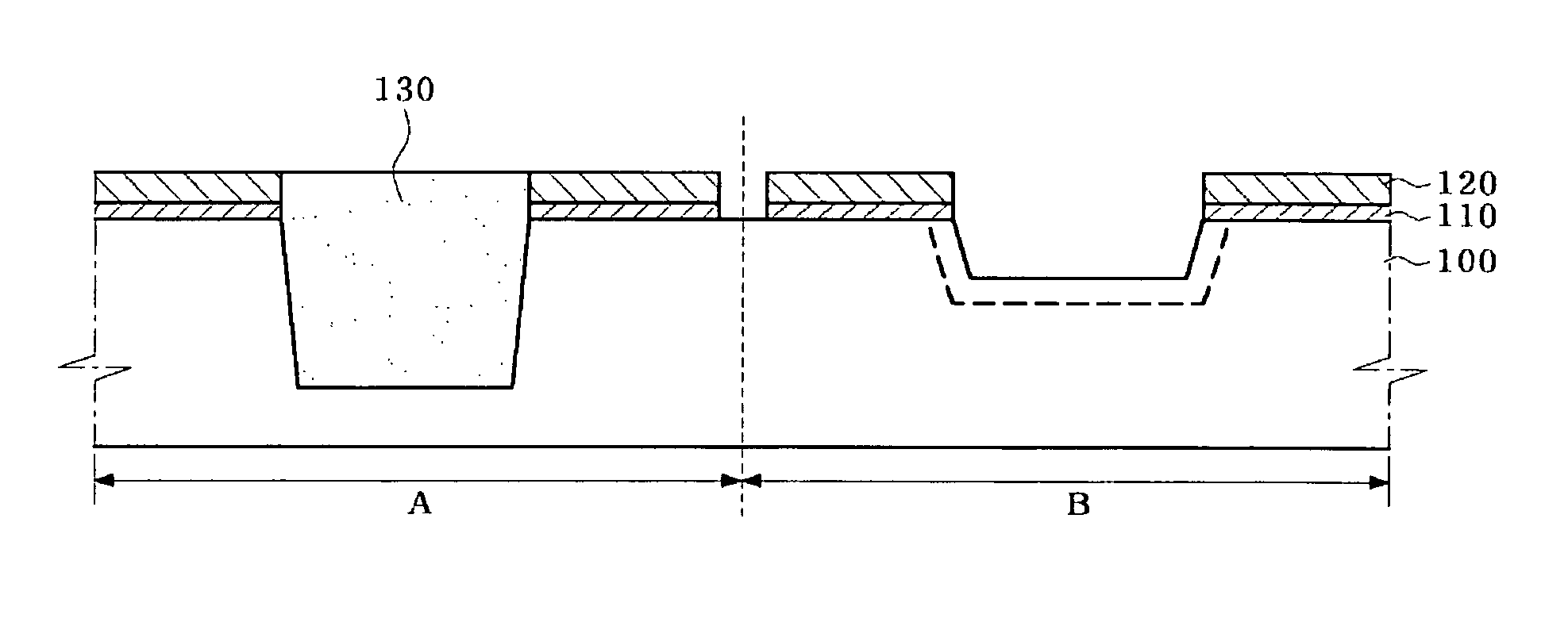
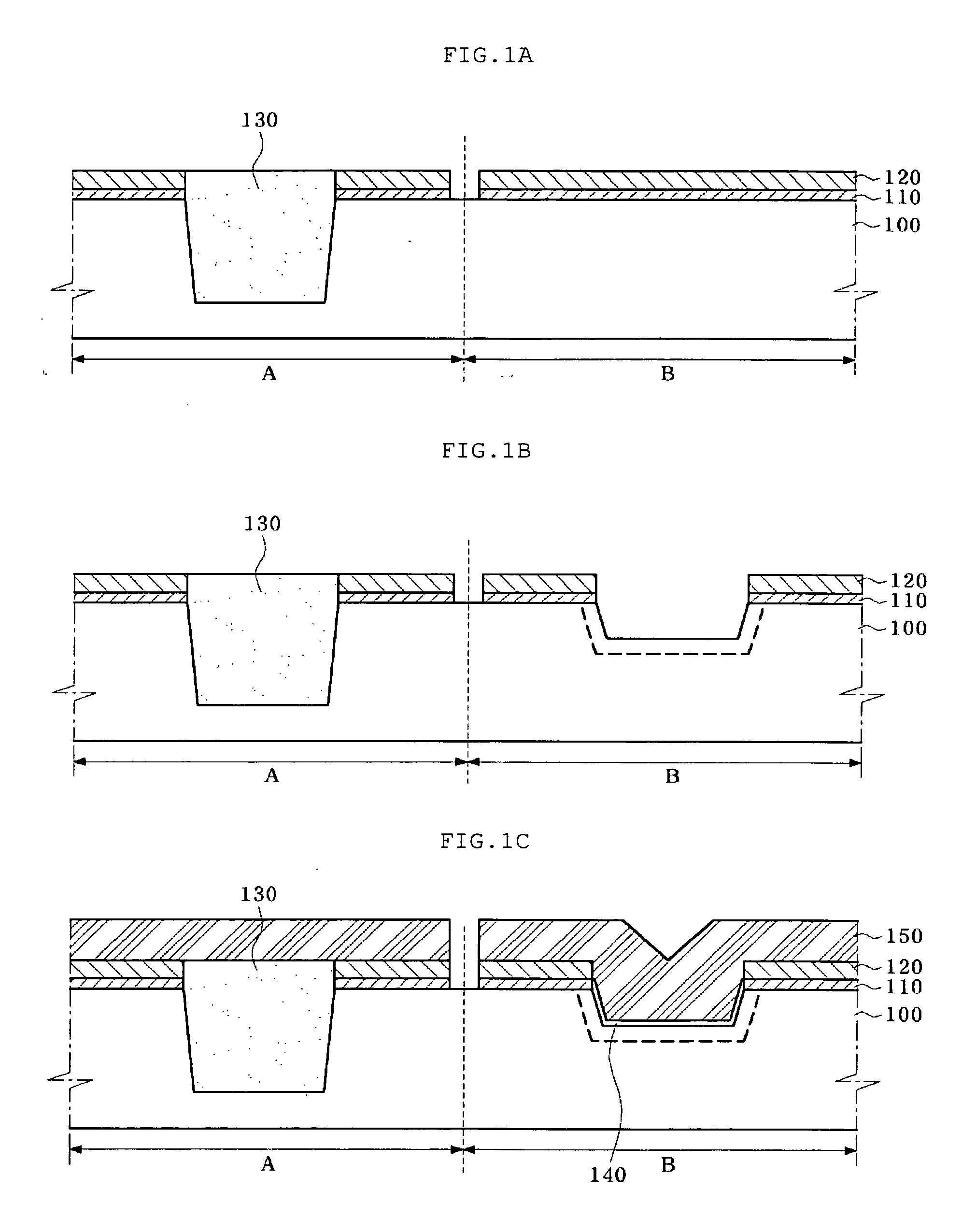
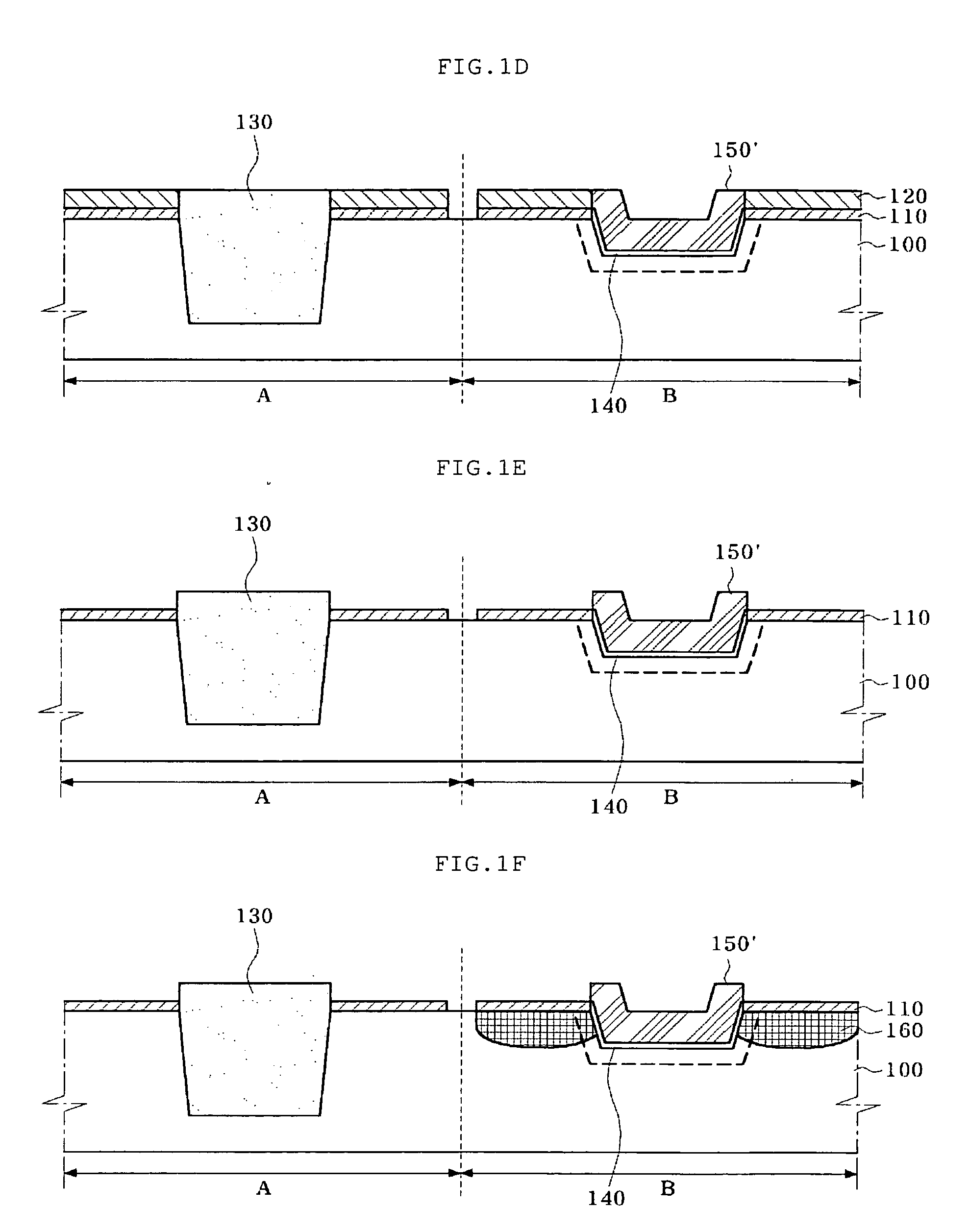
[0017] Firstly, as shown in FIG. 1a, a silicon oxide film 110 and a silicon nitride film 120 are sequentially deposited on a silicon substrate 100 divided into a peripheral circuit region A and cell region B, and then a first trench (not shown) having a first depth is formed on the silicon substrate 100 of the peripheral circuit region A by a photographic process and an etching process. Then, a buried oxide film 130, such as a HDP oxide film or USG (undoped silica glass) film, is deposited so that the first trench can be buried therein and planarized by a chemical mechanical polishing process. ...


PUM


Abstract

A method for manufacturing a non-volatile memory device which can increase the coupling ratio and can avoid affecting the height of a control gate by forming a trench in a cell region and forming a floating gate in a concave shape in the trench is disclosed. The method comprises: forming a first trench having a first depth on a silicon substrate of a peripheral circuit region, burying the same with a buried oxide film and planarizing the same; forming a second trench having a second depth on the silicon substrate of the cell region; carrying out channel ion implantation to the cell region, forming a tunnel oxide film in the second trench and depositing a floating gate material; forming a floating gate by etching the floating gate material; forming a source/drain junction in the cell region; forming wells in the peripheral circuit and cell regions and depositing a dielectric film; depositing a gate material while leaving the dielectric film only in the channel portion of the cell region; and forming a gate in the peripheral circuit region and a control gate in the cell region by etching the gate material.

Description

BACKGROUND OF THE INVENTION [0001] 1. Field of the Invention [0002] The present invention relates to a method for manufacturing a non-volatile memory device, and more particularly, to a method for manufacturing a non-volatile memory device which avoids affecting the height of the control gate by forming a trench in a cell region, forming a floating gate in a concave shape in the trench and making a dielectric film to cover the floating gate. [0003] 2. Description of the Related Art [0004] Non-volatile memory devices can retain their previous data even though their power supplies are interrupted. These non-volatile memory devices include EPROMs capable of being electrically programmed and erased through the irradiation of a UV light and EEPROMs capable of being electrically programmed and erased. Flash memories have a small chip size and excellent program and erase characteristics in the EEPROM. [0005] The non-volatile memory device typically includes a floating gate capable of accum...

Claims


Application Information

Patent Timeline
IPC IPC(8): H01L21/8247H01L27/10H01L27/105H01L27/115H01L29/423H01L29/788H01L29/792
CPCH01L27/105H01L29/42336H01L27/11534H01L27/11526H10B41/43H10B41/40H10B99/00
Inventor LEE, JUNG HWANCHI, SEO YONG
Owner SK HYNIX INC
Why Eureka
Try Eureka