Oxidation method for altering a film structure and CMOS transistor structure formed therewith

a technology of complementary metal oxide semiconductors and transistors, which is applied in the direction of transistors, semiconductor devices, electrical equipment, etc., can solve the problems of increasing the stress of the approach, reducing the drive current, and reducing the desirable approach, so as to reduce the stress. the effect of magnitud

Inactive Publication Date: 2005-05-05
IBM CORP
View PDF10 Cites 40 Cited by
  • Summary
  • Abstract
  • Description
  • Claims
  • Application Information

AI Technical Summary

Benefits of technology

[0009] According to an aspect of the invention, a method is provided for relaxing a stress present in a film contacting a base lay

Problems solved by technology

Some such films, although desirable in some respects, have an undesirable stress present in them.
However, with the advent of new technology this approach is becoming less desirable due to its physical limitations.
However, if that same

Method used


Image

  • Oxidation method for altering a film structure and CMOS transistor structure formed therewith
  • Oxidation method for altering a film structure and CMOS transistor structure formed therewith
  • Oxidation method for altering a film structure and CMOS transistor structure formed therewith

Examples


Embodiment Construction

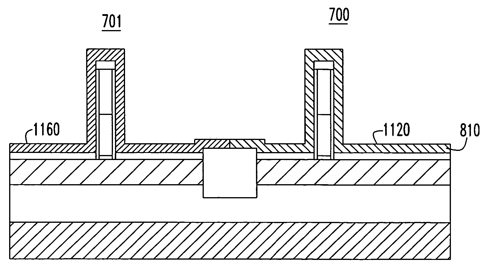
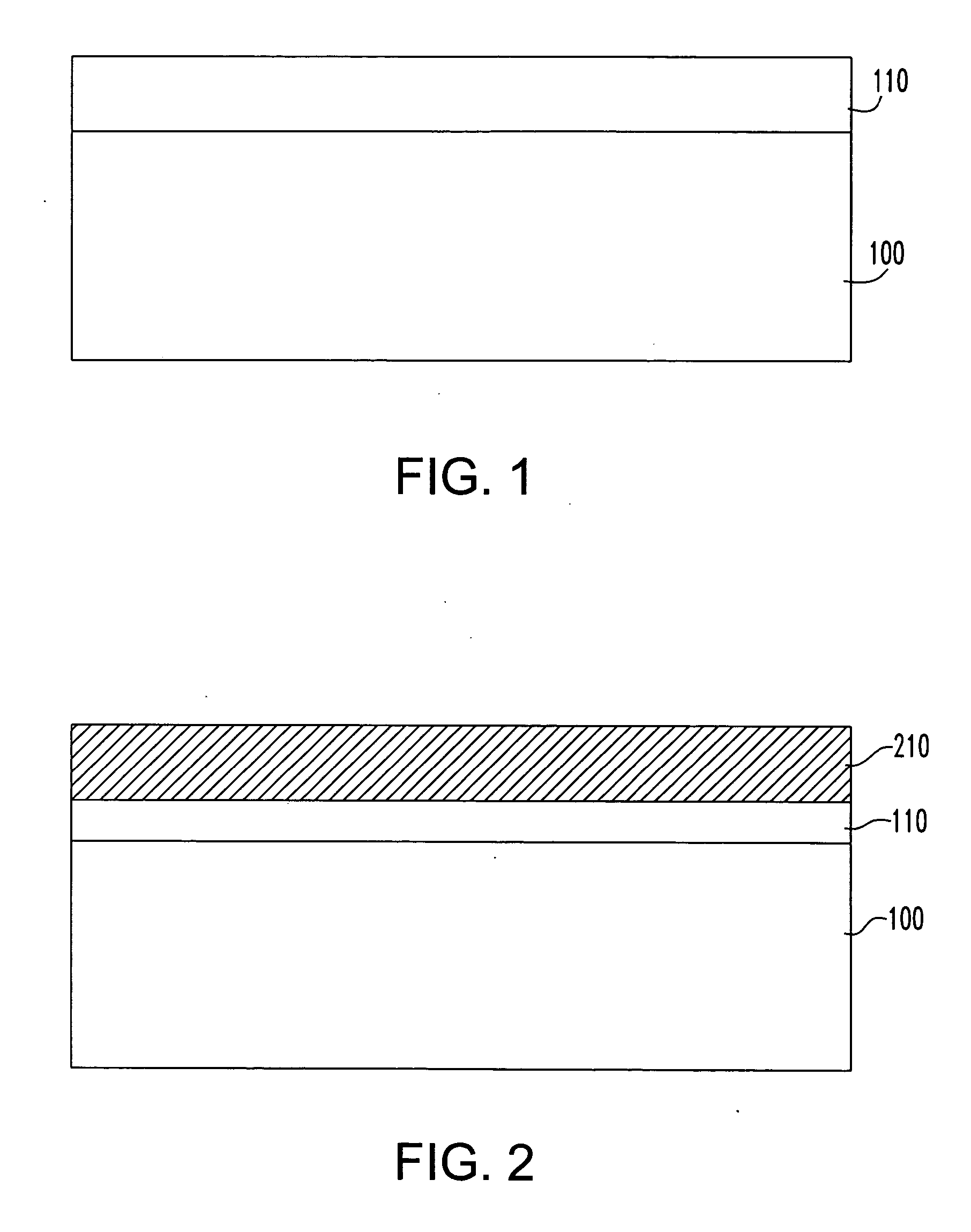
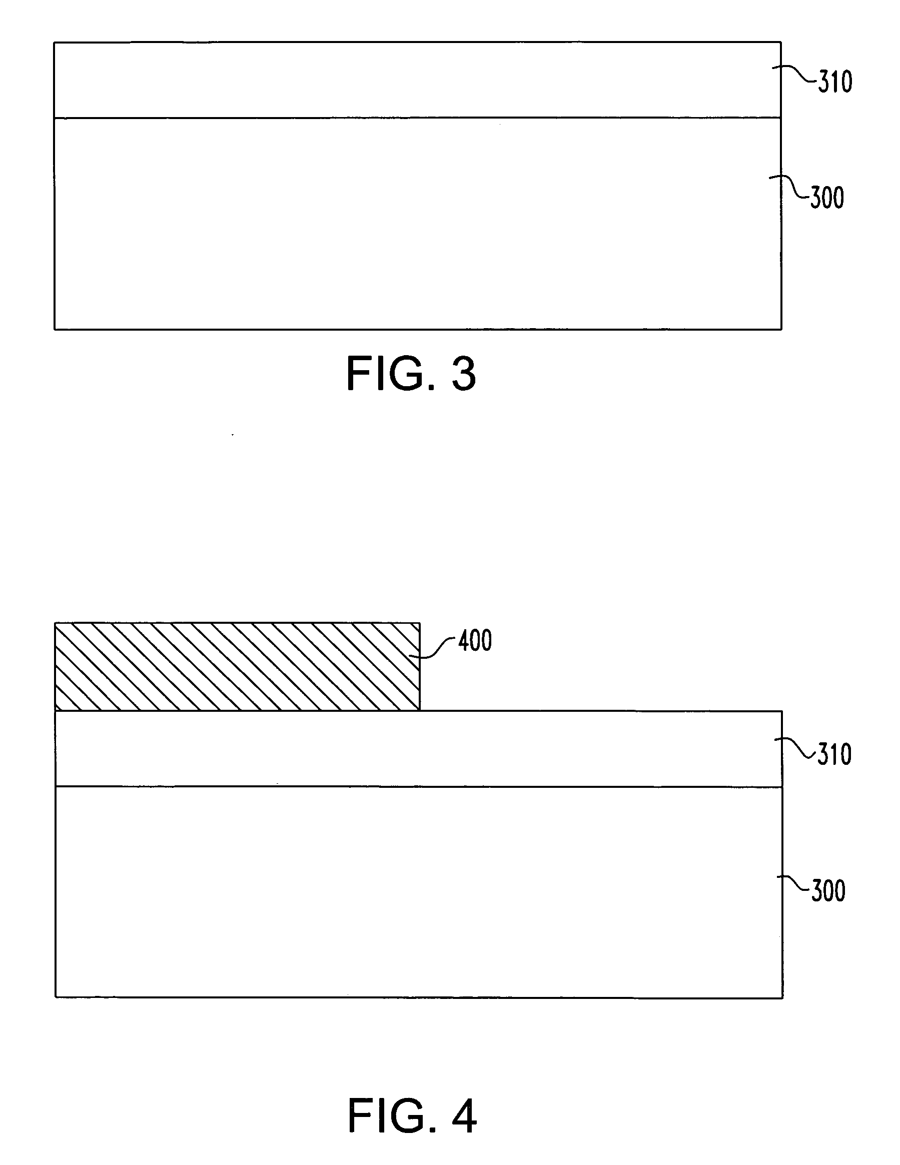
[0018]FIGS. 1 through 14 illustrate stages of a fabrication process according to different embodiments of the present invention. These embodiments as provided in FIGS. 1 and 2; and 3 through 6 provide for the processing and formation of a stressed film that is selectively relaxed in certain areas. FIGS. 7 through 14 focus on the application of the present invention to a CMOS fabrication process having a p-type field effect transistor (PFET) and an n-type field effect transistor (NFET) on a semiconductor substrate or wafer. In the PFET, a stress is applied to the channel region in a first magnitude by a layer of stressed film formed over the source and drain regions. On the other hand, the stress applied to the channel region of the NFET by the film formed over the source / drain regions of the NFET is relaxed. In such manner, an increase in carrier mobility of the PFET is achieved while still maintaining desirable performance in the NFET. Alternatively, the stress applied to the chann...


PUM


Abstract

A structure and method are provided in which a stress present in a film is reduced in magnitude by oxidizing the film through atomic oxygen supplied to a surface of the film. In an embodiment, a mask is used to selectively block portions of the film so that the stress is relaxed only in areas exposed to the oxidation process. A structure and method are further provided in which a film having a stress is formed over source and drain regions of an NFET and a PFET. The stress present in the film over the source and drain regions of either the NFET or the PFET is then relaxed by oxidizing the film through exposure to atomic oxygen to provide enhanced mobility in at least one of the NFET or the PFET while maintaining desirable mobility in the other of the NFET and PFET.

Description

BACKGROUND OF INVENTION [0001] The present invention relates to the fabrication of semiconductor integrated circuits, and more specifically to a method of altering the stress of a thin film and complementary metal oxide semiconductor (CMOS) transistor structures which are formed with such stress altered film. [0002] Thin layers of film are used in the semiconductor industry to alter or enhance the characteristics of adjacent and underlying or base layers. The film may be comprised of a variety of materials chosen selectively to provide certain advantages. Among of the advantages provided by a particular film are a desirable thickness, longevity and dielectric strength, as well as the ability to withstand temperatures. A layer of film can also enhance conformity of deposition of other layers, or provide gap filling characteristics or enhance planarity. Some such films, although desirable in some respects, have an undesirable stress present in them.[0003] However, in certain circumsta...

Claims


Application Information

Patent Timeline
IPC IPC(8): H01L21/8238H01L21/84H01L27/12
CPCH01L21/823807H01L21/823814H01L29/7843H01L27/1203H01L21/84
Inventor BELYANSKY, MICHAEL P.BOYD, DIANE C.DORIS, BRUCE B.GLUSCHENKOV, OLEG
Owner IBM CORP
Why Eureka
Try Eureka