Method for producing optical element having antireflection structure, and optical element having antireflection structure produced by the method

a technology of anti-reflection structure and optical element, which is applied in the direction of electric/magnetic/electromagnetic heating, hollow wall articles, instruments, etc., can solve the problems of low etching rate, and limited optical material that can be used

Inactive Publication Date: 2005-05-05
PANASONIC CORP
View PDF5 Cites 42 Cited by
  • Summary
  • Abstract
  • Description
  • Claims
  • Application Information

AI Technical Summary

Benefits of technology

[0016] A fourth aspect of the present invention is directed to a mold for press-molding heated material for forming an antireflective optical structure, has a substrate having a pattern formed thereon corresponding to the antireflective optical structure to be formed in a material by press-molding; and a thin film formed over the substrate for facilitating removal of the substrate from the material.
[0017] A fifth aspect of the present

Problems solved by technology

However, in the case of micromachining method by dry-etching process, depending on the optical materials to be used, the surface becomes rough after etching, or the etching rate is very low, and therefore the optical material that can be used is limited.
That is to say, the optical material that can be used is limited to quartz glass or the like, and multi component glass or resin, which are used for optical devices that are designed with various optical constants, cannot be used.
Therefore, when it is attempted to produce an optical element having an antireflection structure by micromachining method by dry-etching process, an optical element having an antireflection structure having a large aspect ratio cannot be obtained, because necessary selectivity cannot be obtained.
Furthermore, since the repeatability of etching is low, the yield is reduced, and consequently the production cost is increased significantly.
Therefore, a pattern with fine concavities and convexities cannot be transferred precisely over a large area.
However, when glass serving as the optical material is press-molded, using the mold disclosed in JP62-28091B that is produced

Method used


Image

  • Method for producing optical element having antireflection structure, and optical element having antireflection structure produced by the method
  • Method for producing optical element having antireflection structure, and optical element having antireflection structure produced by the method
  • Method for producing optical element having antireflection structure, and optical element having antireflection structure produced by the method

Examples


first embodiment

[0034] This embodiment will be described by taking a plate optical element having a cone-shaped microstructure of a pitch of 0.15 μm and a depth of 0.15 μm at one face as an example of the optical element having an antireflection structure of the present invention.

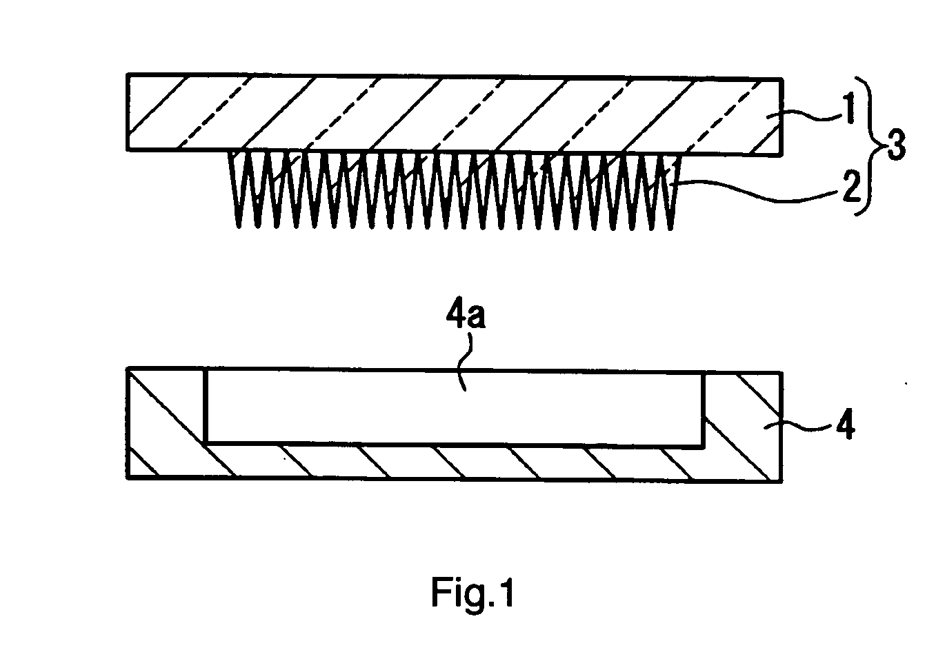
[0035]FIG. 1 is a cross-sectional view showing a mold for press-molding an optical element having an antireflection structure in the first embodiment of the present invention.

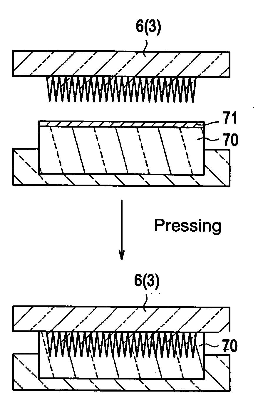
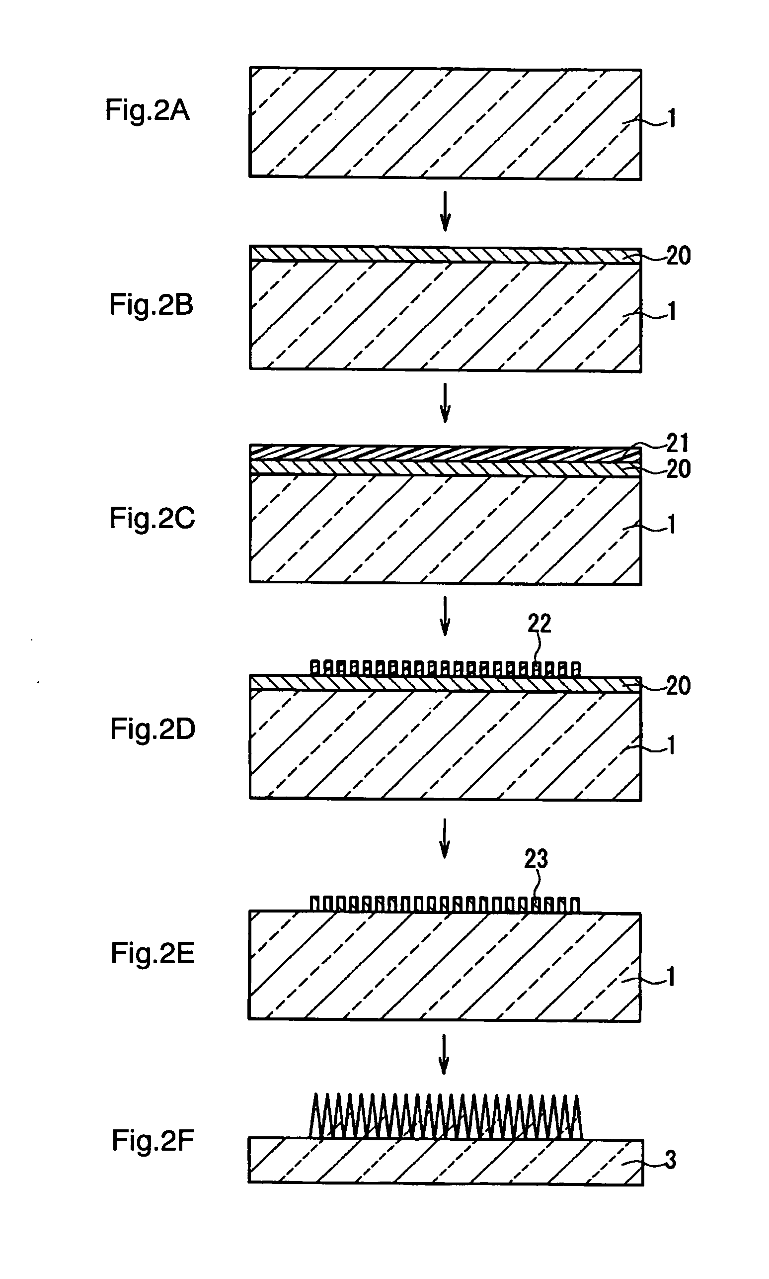
[0036] In FIG. 1, reference numeral 1 denotes a quartz glass substrate of 20 mm×20 mm×5 mm. Quartz glass is a material that has excellent high temperature strength and heat resistance and whose surface is hardly roughened by dry-etching. In the surface (pressing surface) of the quartz glass substrate 1, a cone-shaped antireflection structure 2 having a pitch of 0.15 μm and a height of 0.15 μm is formed, and the quartz glass substrate 1 in which this antireflection structure 2 is formed is used as a mold 3 having an antireflection structure.

[0037] H...

second embodiment

[0051] In this embodiment, substantially the same mold as in the first embodiment was used as the mold for press-molding an optical element having an antireflection structure (see FIG. 1). The mold for press-molding in this embodiment is different from the mold for press-molding in the first embodiment in the following point. In this embodiment, when producing the mold 3 having an antireflection structure, a carbon (C) film for mold release having a thickness of 0.05 μm was formed on the surface (pressing surface) of the quartz glass substrate 1 provided with the cone-shaped antireflection structure 2, instead of forming an Ir—Rh alloy film for protecting the surface. For this reason, in this embodiment, unlike the first embodiment, a releasing agent is not applied onto the surface of the optical material 11 to be press-molded.

[0052] A method for producing the optical element 17 having an antireflection structure, using the mold 3 having an antireflection structure and the lower me...

third embodiment

[0055] In this embodiment, substantially the same mold as in the first embodiment was used as the mold for press-molding the optical element 17 having an antireflection structure (see FIG. 1).

[0056] The process for molding the optical element 17 having an antireflection structure is substantially the same as that in the first embodiment. The molding process in this embodiment is different from the molding process in the first embodiment in the following point. In this embodiment, the optical element 17 having an antireflection structure is molded while N2 and CO2 (10 vol. %) was introduced from an atmosphere gas inlet 18 of the chamber 15 to the inside of the molding machine.

[0057] When the optical element 17 having an antireflection structure was molded in the atmosphere as above, it was found that an optical element 17 having a highly precise antireflection structure without pattern dislocation over the entire area of 15 mm×15 mm of the optical material 11 could be molded repeat...


PUM

PropertyMeasurementUnit
Thicknessaaaaaaaaaa
Diameteraaaaaaaaaa
Heightaaaaaaaaaa

Abstract

A cylinder-shaped Cr mask having a diameter of 0.15 μm is formed at a pitch of 0.15 μm on a quartz glass substrate. The quartz glass substrate on which the cylinder-shaped Cr mask is formed is placed in a RF dry-etching apparatus and the surface of the quartz glass substrate is etched with CHF3+O2 gas. Thus, a cone-shaped antireflection structure with a pitch of 0.15 μm and a height of 0.15 μm is formed on the surface of the quartz glass substrate. An Ir—Rh alloy film having a thickness of 0.05 μm for protecting the surface is formed on the surface (pressing surface) of the quartz glass substrate provided with the cone-shaped antireflection structure to form a mold having an antireflection structure. An optical material 11 (crown based borosilicate glass) to which a releasing agent containing carbon (C) particulates for mold release is applied is press-molded with the mold having an antireflection structure, and the press-molded optical material is released from the mold having an antireflection structure without cooling. After the press-molded optical material is cooled, the releasing agent is removed.

Description

BACKGROUND OF THE INVENTION [0001] 1. Technical Field [0002] The present invention relates to a method for producing an optical element having a highly precise antireflection structure without pattern dislocation over a large area, and the optical element having the antireflection structure produced by this method. [0003] 2. Description of the Background Art [0004] In order to prevent surface reflection of an optical element, it has been proposed to form an antireflection structure on a surface of an optical element. The proposed antireflection structure has very fine concavities and convexities having an aspect ratio of 1 or more at sub-micron pitches. As a method for forming such a fine structure, micromachining method by dry-etching process has been proposed. [0005] On the other hand, a method of press-molding an optical material (deformable material) made of glass or resin has been proposed as an effective method for producing highly precise optical elements in a large amount an...

Claims


Application Information

Patent Timeline
IPC IPC(8): C03B11/08C03C15/00C03C17/06G02B5/00
CPCC03B11/082C03B11/086C03B2215/10G02B5/003C03B2215/412C03C15/00C03C17/06C03B2215/17Y02P40/57
Inventor UMETANI, MAKOTOSHIMIZU, YOSHIYUKIYAMAMOTO, YOSHIHARUYAMAGATA, MICHIHIROTANAKA, YASUHIROYAMAGUCHI, HIROSHI
Owner PANASONIC CORP
Why Eureka
Try Eureka