Integrated circuit and method for interfacing two voltage domains using a transformer

a technology of integrated circuits and transformers, applied in the direction of generating/distributing signals, pulse techniques, instruments, etc., can solve the problems of system timing failure, excessive clock jitter, system timing failure, etc., and achieve the effect of reducing on-chip noise coupling

Inactive Publication Date: 2005-05-05
IBM CORP
View PDF4 Cites 5 Cited by
  • Summary
  • Abstract
  • Description
  • Claims
  • Application Information

AI Technical Summary

Benefits of technology

[0008] Another aspect of the present invention is an integrated circuit designed to reduce on-chip noise coupling. The integrated circuit includes the following: a circuit transformer capable of converting a noise sensitive input signal to an output signal having a voltage compatible with a predetermined sink voltage logic level; and a biased receiver transistor network having a PFET current mirror coupled with a NFET current mirror. The biased receiver transistor network is designed to multiply the transformer output signal to offset a mutual coupling loss of the transformer.
[0009] Still another aspect of the present invention is an integrated circuit designed to reduce on-chip noise coupling. The integrated circuit includes the following: means for converting a noise sensitive input signal to an output signal having a voltage compatible with a predetermined sink voltage logic level; and means for multiplying the transformer output signal to offset a mutual coupling loss of the transformer.

Problems solved by technology

Excessive clock jitter can be catastrophic and lead to system timing failures.
One of the leading contributors to clock jitter is electrical noise, which can manifest itself as a delay variation in the PLL feedback loop, transient power bus or substrate noise at the PLL itself, or variations in the edge displacement of the (input) reference clock signal.
As a result, electrical noise 27 in prior art designs may cause excessive clock jitter.

Method used


Image

  • Integrated circuit and method for interfacing two voltage domains using a transformer
  • Integrated circuit and method for interfacing two voltage domains using a transformer
  • Integrated circuit and method for interfacing two voltage domains using a transformer

Examples


Embodiment Construction

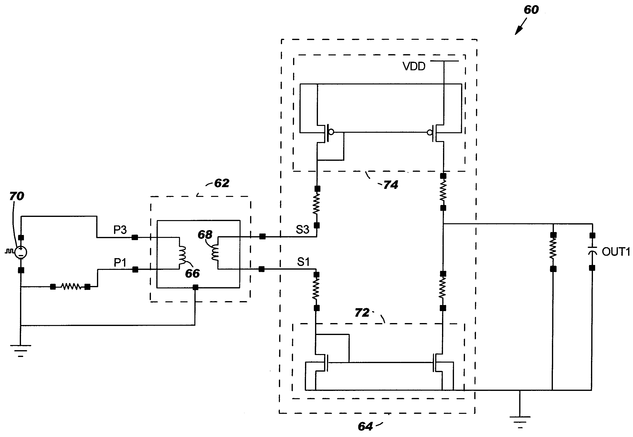
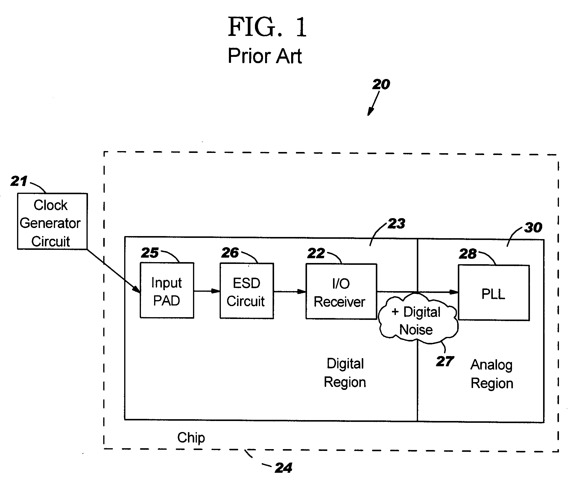
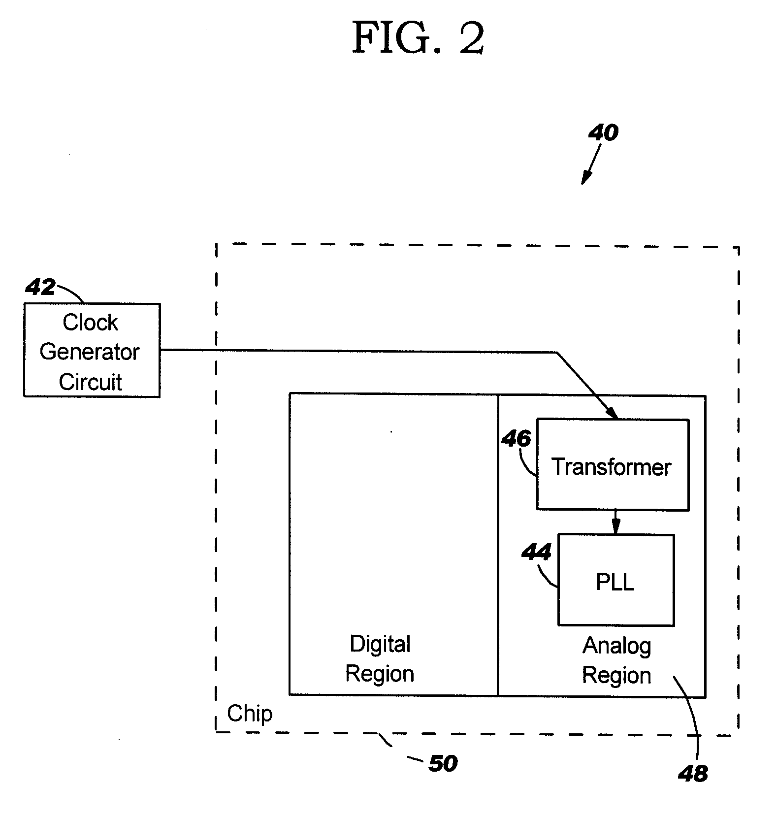
[0017] The present invention is directed to an integrated circuit and method for maintaining the integrity of an input reference clock signal in the presence of a noisy chip environment. An example of the disclosed invention is depicted in FIGS. 2 and 3, although it should be understood that the present invention is not limited to this (or any other) particular embodiment, but rather is intended to cover any integrated circuit or method that fairly falls within the broad scope of the appended claims. In the drawings, like elements include like element numbers.

[0018] Referring now to the drawings, FIG. 2 illustrates a simplified schematic of a circuit design 40 according to one embodiment of the present invention. An off-chip clock generator circuit 42 supplies a reference clock signal (not shown), which is translated to the input of a PLL 44 via a circuit transformer 46, which provides significant and effective physical isolation between its primary and secondary windings (also not...


PUM


Abstract

An integrated circuit designed to reduce on-chip noise coupling. In one embodiment, circuit (60) includes the following: a circuit transformer (62) capable of converting a noise sensitive input reference clock signal to an output signal having a voltage compatible with a predetermined sink voltage logic level; and a biased receiver network (64) having a PFET current mirror (74) coupled with a NFET current (72), the biased receiver transistor network designed to multiply the transformer signal to offset a mutual coupling loss of the transformer. In at least one alternative embodiment, the input reference clock signal originates at an off-chip clock generator circuit (42) and the output signal from receiver (64) is input to a PLL (44). In another alternative embodiment, the transformer is a monolithic integrated transformer. Another alternative embodiment of the present invention is a method of reducing on-chip noise coupling.

Description

BACKGROUND OF INVENTION [0001] 1. Field of the Invention [0002] The present invention relates generally to an integrated circuit and method for interfacing two voltage domains using a transformer, and more particularly to an integrated circuit and method for maintaining the integrity of an input reference clock signal in the presence of a noisy chip environment. [0003] 2. Background of the Invention [0004] Phase-locked loops (PLLs) are analog circuits that are employed extensively in on-chip clock generation and redistribution systems. PLLs use phase / frequency correction to generate chip clock waveforms that in some way mimic the characteristics of an input reference clock signal. Ideally, the edges of the PLL-generated clock waveform are distributed to be precisely periodic, i.e., the duration of successive clock cycles are constant. Deviation from this ideal behavior is measured using a figure-of-merit called “clock jitter”. Excessive clock jitter can be catastrophic and lead to s...

Claims


Application Information

Patent Timeline
Patent Type & Authority Applications(United States)
IPC IPC(8): H01L27/02H03K17/691H03K19/0175
CPCH01L27/0251H03K19/017545H03K17/691
Inventor HO, SHIU CHUNGWEMPLE, IVAN L.WYATT, STEPHEN D.
Owner IBM CORP
Why Eureka
Try Eureka