Optical reduction system with elimination of reticle diffraction induced bias

Inactive Publication Date: 2005-05-05
SILICON VALLEY GRP INC
View PDF14 Cites 5 Cited by
  • Summary
  • Abstract
  • Description
  • Claims
  • Application Information

AI Technical Summary

Benefits of technology

[0007] While these optical systems perform adequately for their intended purpose, there is an ever increasing need to improve system performance. The present inventor has identified that a need exists for

Problems solved by technology

Variations on the wafer affect the performance of the semiconductor device, an

Method used


Image

  • Optical reduction system with elimination of reticle diffraction induced bias
  • Optical reduction system with elimination of reticle diffraction induced bias
  • Optical reduction system with elimination of reticle diffraction induced bias

Examples


example implementations

III. Example Implementations

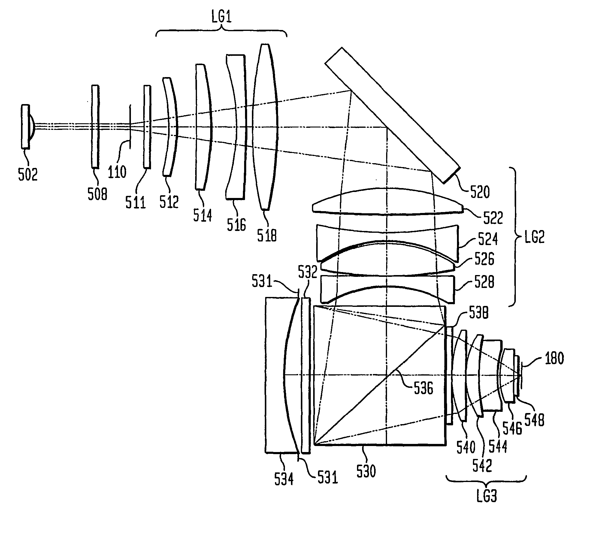
[0031] A. Optical System With Elimination of Reticle Diffraction Induced Bias

[0032] B. Alternate Embodiment

[0033] C. Further Embodiments

IV. Alternate Implementation

I. Overview

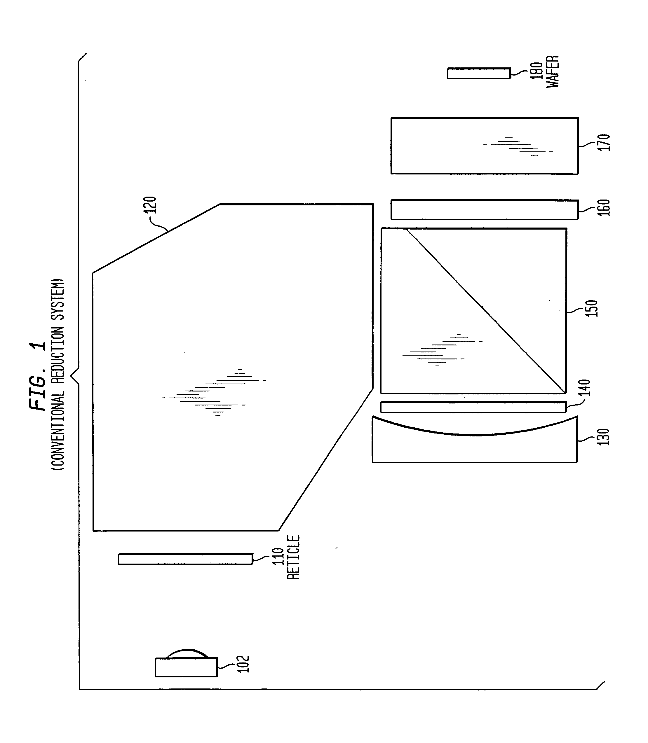
[0034] A. Conventional Optical System

[0035]FIG. 1 illustrates a conventional optical reduction system. From its long conjugate end where the reticle is placed to its short conjugate end where the wafer is placed, it possesses a first optical component group 120, a beamsplitter cube 150, a first quarter-wave plate 140, a concave mirror 130, a second quarter-wave plate 160, and a second optical component group 170. A feature of any optical system is the interdependence of numerical aperture size and spectral radiation requirements. In order to efficiently illuminate the image or wafer plane 180, linearly polarized light is used. The limitations of linearly polarized light are introduced above and discussed in the following sections.

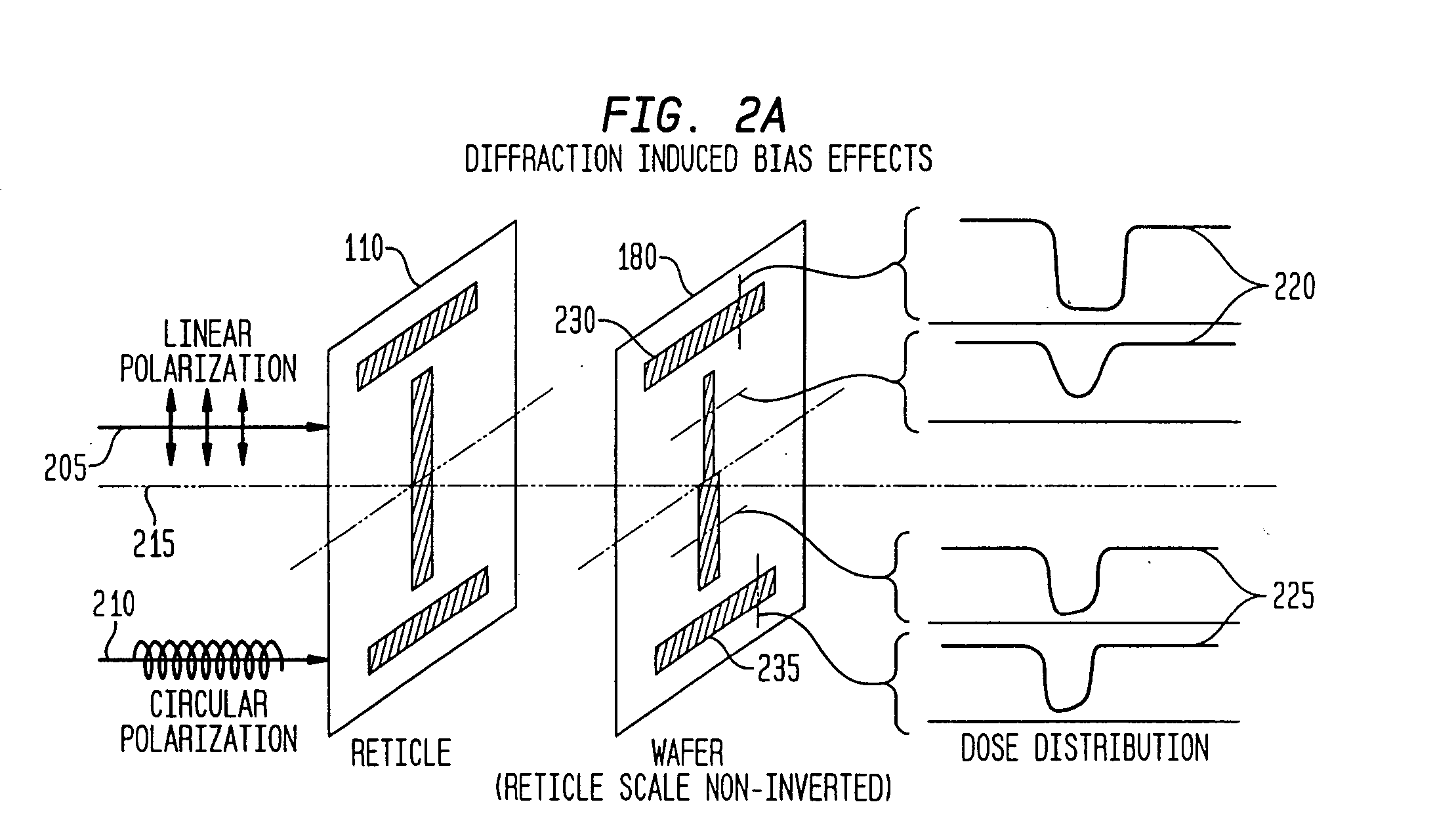
[0036] B. Reticle Diffraction Induced Bias

[0...


PUM


Abstract

An optical reduction system for use in the photolithographic manufacture of semiconductor devices having one or more quarter-wave plates operating near the long conjugate end. A quarter-wave plate after the reticle provides linearly polarized light at or near the beamsplitter. A quarter-wave plate before the reticle provides circularly polarized or generally unpolarized light at or near the reticle. Additional quarter-wave plates are used to further reduce transmission loss and asymmetries from feature orientation. The optical reduction system provides a relatively high numerical aperture of 0.7 capable of patterning features smaller than 0.25 microns over a 26 mm×5 mm field. The optical reduction system is thereby well adapted to a step and scan microlithographic exposure tool as used in semiconductor manufacturing. Several other embodiments combine elements of different refracting power to widen the spectral bandwidth which can be achieved.

Description

CROSS REFERENCE TO RELATED APPLICATIONS [0001] This application is a continuation of U.S. Pat. appl. Ser. No. 10 / 366,614, filed Feb. 14, 2003, which is a continuation of U.S. Pat. Appl. Ser. No. 09 / 841,166, filed Apr. 25, 2001, which claims the benefit of U.S. Provisional Pat. Appl. No. 60 / 199,392, filed Apr. 25, 2000, each of which is hereby incorporated by reference herein in its entirety.BACKGROUND OF THE INVENTION [0002] 1. Field of the Invention [0003] This invention relates generally to optical systems used in semiconductor manufacturing. [0004] 2. Background Art [0005] Semiconductor devices are typically manufactured using various photolithographic techniques. The circuitry used in a semiconductor chip is projected from a reticle onto a wafer. This projection is often accomplished with the use of optical systems. The design of these optical systems is often complex, and it is difficult to obtain the desired resolution necessary for reproducing the ever-decreasing size of comp...

Claims


Application Information

Patent Timeline
IPC IPC(8): G02B17/08G03F7/20G03F7/22H01L21/027
CPCG03F7/70225G03F7/70566G03F7/70358G03F7/70308H01L21/027
Inventor KREUZER, JUSTIN L.
Owner SILICON VALLEY GRP INC
Why Eureka
Try Eureka