Method and apparatus for manufacturing organic EL display and color filter by ink jet method

a technology of organic electroluminescence and ink jet, which is applied in the field of information display, can solve the problems of large influence, deterioration of light-emitting materials, and inability to achieve the effect of making film thickness even by forcible drying, and achieves excellent practice, high material usability, and sufficient brightness.

Inactive Publication Date: 2005-05-12
DAI NIPPON PRINTING CO LTD
View PDF14 Cites 68 Cited by
  • Summary
  • Abstract
  • Description
  • Claims
  • Application Information

AI Technical Summary

Benefits of technology

[0023] The present application has been accomplished in view of the above mentioned point, and the object is to provide a method and apparatus in which an uniform thickness EL layer is formed, a pixel opening emits light effectively, and an organic EL display having sufficient brightness and excellent in practice is manufactured by an ink jet method. The further object thereof is to provide a method and apparatus for manufacturing a color filter excellent in practice, by an ink jet method, in which an uniform thickness dye layer is formed and optical colorization of uniform color tone is conducted at a pixel opening.
[0024] The present invention is a method for manufacturing an organic EL display by an ink jet method, wherein an uniform organic EL layer is formed by sequentially continuously carrying out: a process of discharge-placing an organic EL material in the form of solution on a substrate; and a process of drying the organic EL material in the form of ink placed on the substrate by heating, and also a method for manufacturing where in the organic EL material is dried by heating over thereof. Further, the present invention is a method for manufacturing an organic EL display wherein the placing of the organic EL material on the substrate and drying by heating are sequentially continuously carried out by relatively moving the substrate to a nozzle which discharges the organic EL material and to a heating device which heats the organic EL material over thereof. By these methods for manufacturing, a problem of uneven thickness of the EL layer can be solved.
[0025] When an organic EL display or a color filter is manufactured by an ink jet method, by employing the present invention, flattening of an organic EL layer and a color filter coloring layer can be easily achieved, and an organic EL display and a color filter with high material usability and excellent property uniformity can be provided.

Problems solved by technology

Since LCD utilizes polarization control by double refraction of liquid crystal, there is so-called strong visibility angle dependency, which display condition varies significantly depending on observing direction, while in the case of a display of self light emitting type, this problem scarcely happens.
In the JP-A No. 11-339957, as solution of a light emitting material, a substrate is heat-dried or vacuum-heat-dried after removal of a solvent at room temperature after discharging onto a substrate, however, after a solvent is removed to a certain degree, no effect of making film thickness even by forcible drying is obtained.
However, removing of a solvent of high boiling point completely cannot avoid a problem that heating treatment at higher temperature is necessary, leading to deterioration of a light emitting material.
Though deterioration is not observed in the initial light emitting property, this problem exerts a large influence particularly on shortening of light emitting life.
If heating treatment is not conducted at sufficient high temperature, a problem of heat deterioration of a light emitting layer will not occur, however, its leads to significant deterioration of the reliability of a light emitting layer due to the remaining of a solvent in a light emitting layer formed as a film.
In the JP-A No. 2001-85161, heating treatment is conducted at higher temperature than the softening point of a material of a light emitting layer, to form a light emitting layer, and there is a problem of deterioration of a light emitting material as described above.
However, this only blows the dried solvent vapor, and the drying is not compulsive.
This may have an effect of improving drying uniformity within the substrate surface, but there is no description about improving the uniformity of stereoscopic film thickness within a pixel, further, they are even not aware of a problem on this case.
When only the pixel center portion emits light as described above, brightness and efficiency sufficient as a display cannot be attained.
Otherwise, a problem of disconnection of facing electrodes is also important.
Usually, since a facing electrode is formed by vapor depositing a metal thin film, thickness from 100 nm to at most 500 nm is a limitation for stable formation.
When thicker than this, a risk of peeling increases due to the tension of a metal itself since it is no longer a thin film.
However, a problem of uneven thickness of an EL layer caused by a meniscus phenomenon is not solved.
The problem of uneven thickness due to a meniscus phenomenon occurs not only in an EL light emitting layer but also in other functional layers, for example, a hole injection layer, hole transportation layer, electron injection layer and electron transportation layer when formed from a solution.
However, as shown in FIG. 17, there is a problem that flattening of a dye layer is difficult, same as in the case of an organic EL material described above.
Therefore, when the film thickness is still uneven as shown in FIG. 17, it will be a color filter having irregularity and useless.

Method used


Image

  • Method and apparatus for manufacturing organic EL display and color filter by ink jet method
  • Method and apparatus for manufacturing organic EL display and color filter by ink jet method
  • Method and apparatus for manufacturing organic EL display and color filter by ink jet method

Examples


example 1

[0084] The following solution was prepared as an example of the present invention.

[0085] (Preparation of Organic EL Layer Forming Coating Solution)

Polyvinylcarbazole70 parts by weightOxadiazole compound30 parts by weightCoumarin 6 (* fluorescent dye) 1 part by weight

[0086]

* When the fluorescent dye is coumarin 6, green light emission having a peak at 501 nm, in the case of perylene, blue light emission having a peak at 460 to 470 nm, and in the case of DCM, red light emission having a peak at 570 nm was obtained, and these were used as light emitting materials of each color.

[0087] These were dissolved in a proportion of 0.5 wt % in tetralin (solvent), to produce an organic EL material ink for ink jet.
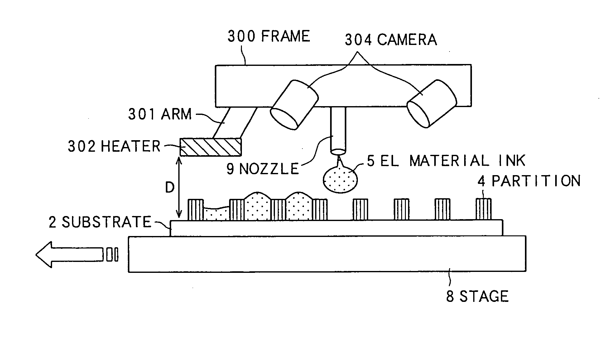
(Ink Jet Apparatus)

[0088] An ink jet apparatus provided with functions for discharging ink and continuously drying by heating over thereof as shown in FIG. 1 was fabricated. An IR heater was used for heating. The distance between a nozzle and a substrate, also, a distance between...

example 2

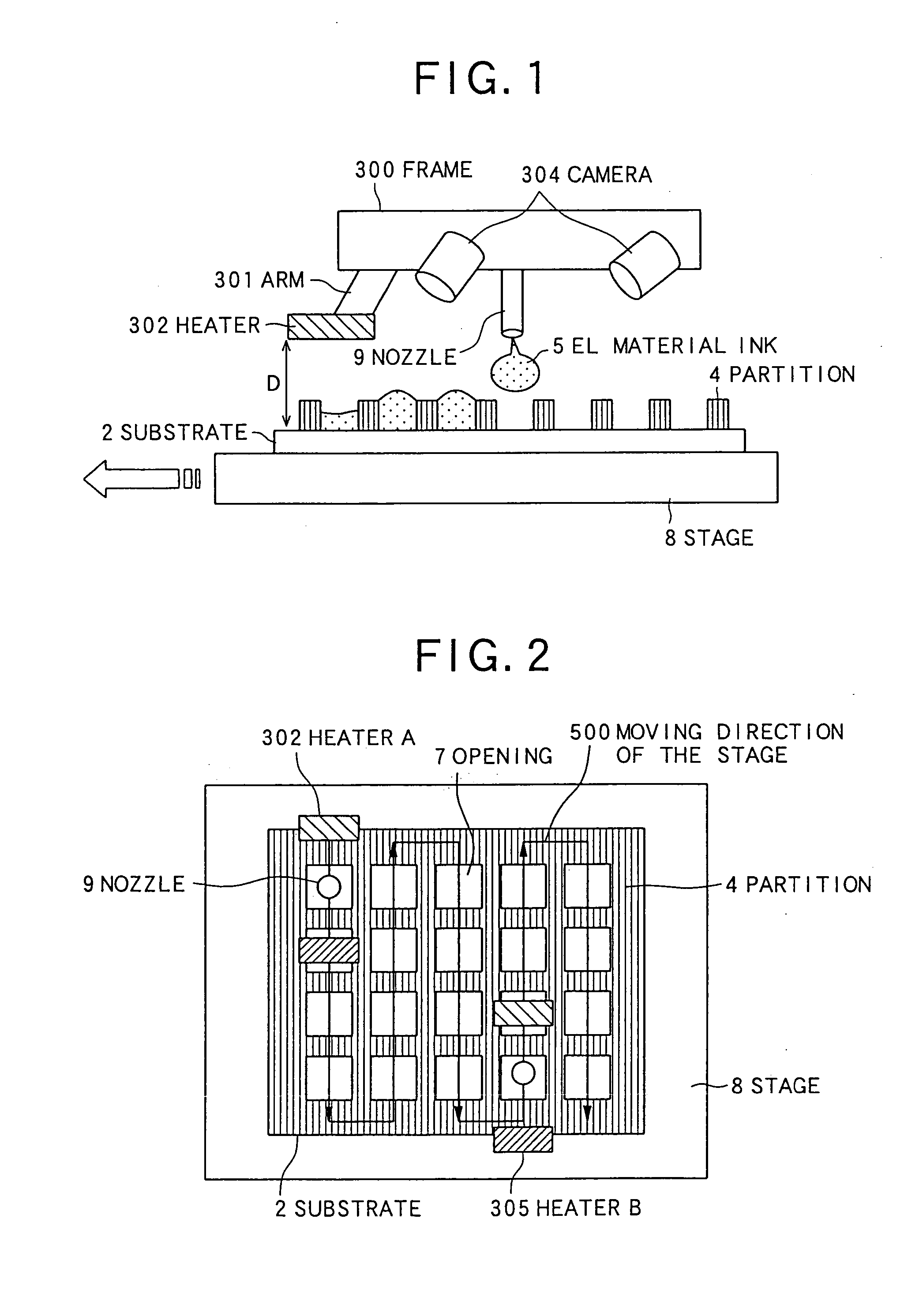
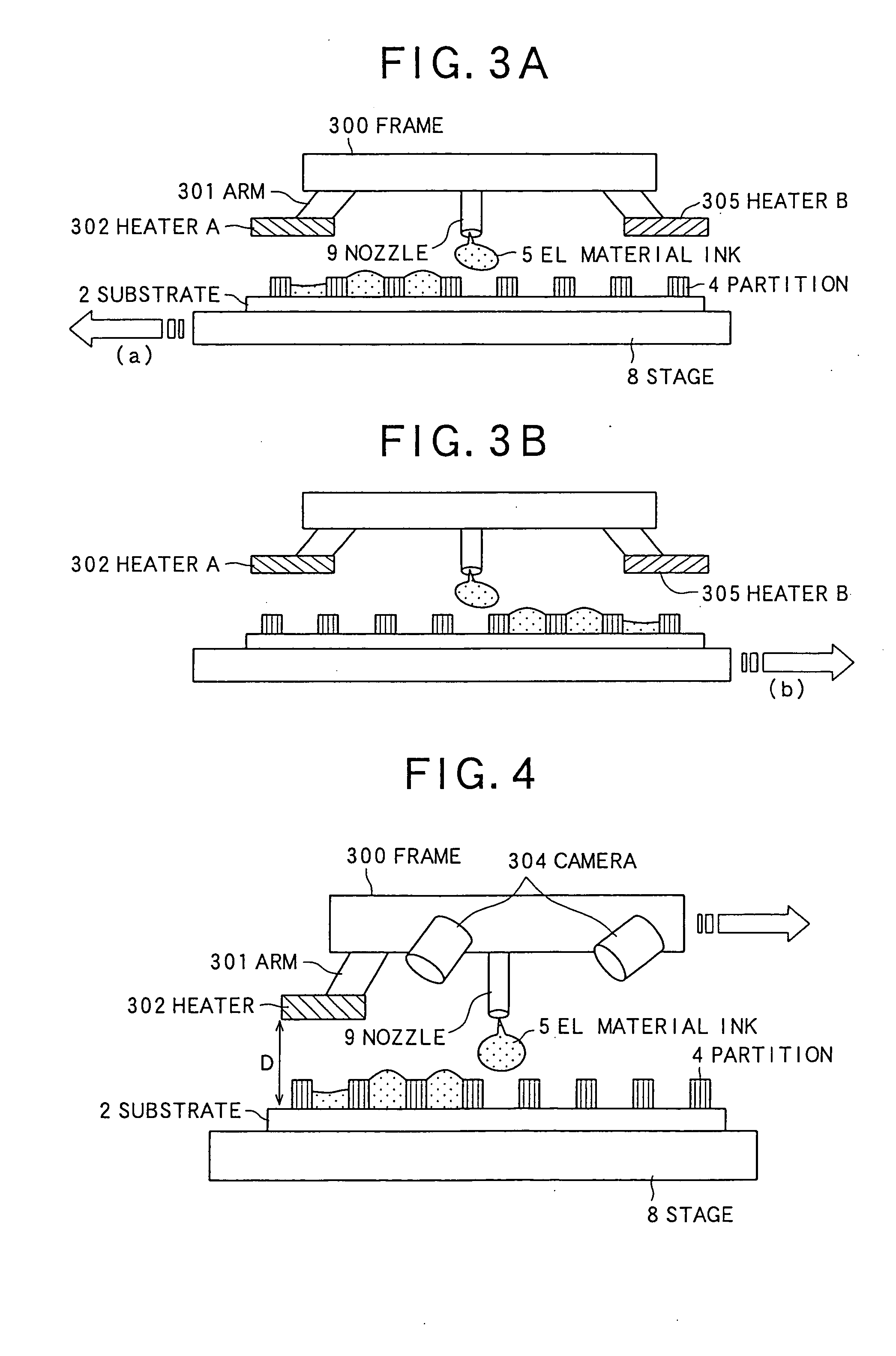
[0096] The same procedure as in Example 1 was conducted except that the ink jet apparatus of Example 1 was improved by providing heaters on the both sides of the nozzle as shown in FIG. 3, the movement of the stage was made into a combination of reciprocation and parallel movement as shown in FIG. 2, and ink discharge and drying by heating was carried out so that the heater at the backward of the nozzle, relatively to the stage reciprocation, is on.

[0097] When a control circuit was connected to thus manufactured organic EL display and image signals were applied to drive the apparatus, poor emission derived from uneven thickness of an EL layer as shown in FIG. 12 did not occur, and uniform and bright color image display could be conducted on the entire surface, as in Example 1.

[0098] In Example 1, drying by heating could be carried out when the stage is moving in only one direction. However, drying by heating can be carried out when the stage is moving in either direction of the re...

example 3

[0099] The same procedure as in Example 1 was conducted except, as shown in FIG. 4, a stage was fixed, and mechanisms for X (longitudinal), Y (lateral), Z (up and down) and θ (rotation) and motors were provided so that a head portion could move in any directions, and an organic EL display capable of conducting uniform and bright color image display on the entire surface as in Example 1 could be manufactured.


PUM

PropertyMeasurementUnit
heightaaaaaaaaaa
thicknessaaaaaaaaaa
thicknessaaaaaaaaaa

Abstract

The object of the present invention is to provide a method and apparatus for manufacturing an EL layer of uniform thickness, causing effective light emission of pixel openings and manufacturing an organic EL display showing sufficient brightness and excellent in practicability, by an ink jet method. Further object is to provide a method and apparatus for manufacturing a color filter excellent in practicability by an ink jet method, in which a dye layer with uniform thickness is formed and optical coloring of uniform tone is conducted at pixel openings. In order to achieve the above object, the present invention is a method for manufacturing an organic EL display by an ink jet method, wherein an uniform organic EL layer is formed by sequentially continuously carrying out: a process of discharge-placing at least an organic EL material in the form of solution on a substrate; and a process of drying the organic EL material in the form of ink placed on the substrate by heating, and the organic EL material is dried by heating over thereof. Further, the placing of the organic EL material on the substrate and drying by heating are sequentially continuously carried out by relatively moving the substrate to a nozzle which discharges the organic EL material and to a device which heats the organic EL material over thereof.

Description

BACKGROUND OF THE INVENTION [0001] 1. Field of the Invention [0002] The present invention relates to an information display. Particularly, the present invention relates to a method and apparatus for manufacturing an organic electroluminescence (EL) display. Further, the present invention relates to a method and apparatus for manufacturing a color filter. [0003] 2. Description of the Related Art [0004] Recently, flat displays are used in many fields and places, and the importance is growing with the progressing of computerization. Nowadays, the typical examples of flat displays are liquid crystal displays (LCD), however, as flat displays based on a different display mode from that of LCD, organic EL, inorganic EL, plasma display panels (PDP), light emitting diode displays (LED), vacuum fluorescent displays (VFD), field emission displays (FED), and the like are being actively developed. These new flat displays are all called a display of self light emitting type, and are significantly...

Claims


Application Information

Patent Timeline
Patent Type & Authority Applications(United States)
IPC IPC(8): H01L27/32H01L51/00H01L51/40H01L51/56
CPCH01L27/322H01L51/0005H01L51/007H01L51/0042H01L51/0065H01L51/0037H10K59/38H10K71/135H10K85/146H10K85/1135H10K85/653H10K85/6565
Inventor ITO, NOBUYUKIITO, NORIHITO
Owner DAI NIPPON PRINTING CO LTD
Why Eureka
Try Eureka