Etching method and plasma etching apparatus

a plasma etching and etching method technology, applied in the direction of electrical equipment, basic electric elements, electric discharge tubes, etc., can solve the problems of insufficient etching of holes, and tapered side walls of holes as formed, etc., to achieve low plasma density, low etching selection ratio, and small contribution of ion energy

Inactive Publication Date: 2005-05-19
TOKYO ELECTRON LTD +1
View PDF21 Cites 21 Cited by
  • Summary
  • Abstract
  • Description
  • Claims
  • Application Information

AI Technical Summary

Benefits of technology

[0019] According to the result of investigation executed by inventors of the present invention, in case of etching a film made of an organic material (resist), the plasma density plays a dominant part while contribution of the ion energy is small. On one hand, in order to make the etching selection ratio high when etching a film made of an inorganic material (e.g. silicon oxide film), it is necessary to make the plasma density low as well as to make the ion energy high. In this case, since it is possible to indirectly grasp the plasma ion energy by means of a self-bias voltage at the electrode at the time of etching, in order to etch the silicon oxide film at a high etching rate as well as at high etching selection ratio, it is effective to carry out an etching process under the condition of a low plasma density and a high self-bias voltage. If the frequency of the high frequency power applied to the electrode becomes high, a desired plasma density can be obtained with the low power, so that the power consumption is reduced to a great extent.
[0021] According to the etching method of the invention like this, by executing the etching process at the low plasma electron density as well as at the high self-bias voltage, it becomes possible to make the etching rate of the etching target film large as well as to make the etching selection ratio of the etching target film relative to the mask material film large. Accordingly, it becomes possible to provide the etching target material with fine holes of which each has a flat smooth side surface approximately vertical to the workpiece surface and a bottom area secured enough relative to the entrance opening area of the hole.
[0029] According to the etching apparatus of the invention like this, by executing the etching process by means of the low plasma electron density and the high self-bias voltage, it is become possible to make the etching rate of the etching target film large as well as to make the etching selection ratio of the etching target film relative to the mask material film large. Accordingly, it becomes possible to provide the etching target material with fine holes of which each has a flat smooth side surface approximately vertical to the workpiece surface and a bottom area secured enough relative to the opening area of the hole.
[0036] According to the etching method of the invention like this, by executing the etching process by means of the low plasma electron density and the high self-bias voltage, it is become possible to make the etching rate of the etching target film large as well as to make the etching selection ratio of the etching target film relative to the mask material film large. Accordingly, it becomes possible to provide the etching target material with fine holes of which each has a flat smooth side surface approximately vertical to the workpiece surface and a bottom area secured enough relative to the entrance opening area of the hole.
[0044] According to the etching apparatus of the invention like this, by executing the etching process by means of the low plasma electron density and the high self-bias voltage, it is become possible to make the etching rate of the etching target film large as well as to make the etching selection ratio of the etching target film relative to the mask material film large. Accordingly, it becomes possible to provide the etching target material with fine holes of which each has a flat smooth side surface approximately vertical to the workpiece surface and a bottom area secured enough relative to the entrance opening area of the hole.

Problems solved by technology

However, when executing the fine and sophisticated etching process by means of the above-mentioned prior art plasma etching apparatus 10 or 20, since the adequate etching selection ratio of a processing target material relative to a mask material can not be secured enough, there is caused such a problem that a hole having a sufficient depth can not be obtained by etching.
Even if trying to improve this, there are caused other problems, for example, a problem that the bottom area of a hole can not be adequately obtained relative to the entrance opening area of the hole, a problem that the side wall of a hole as formed becomes tapered, and so forth.

Method used


Image

  • Etching method and plasma etching apparatus
  • Etching method and plasma etching apparatus
  • Etching method and plasma etching apparatus

Examples


first embodiment

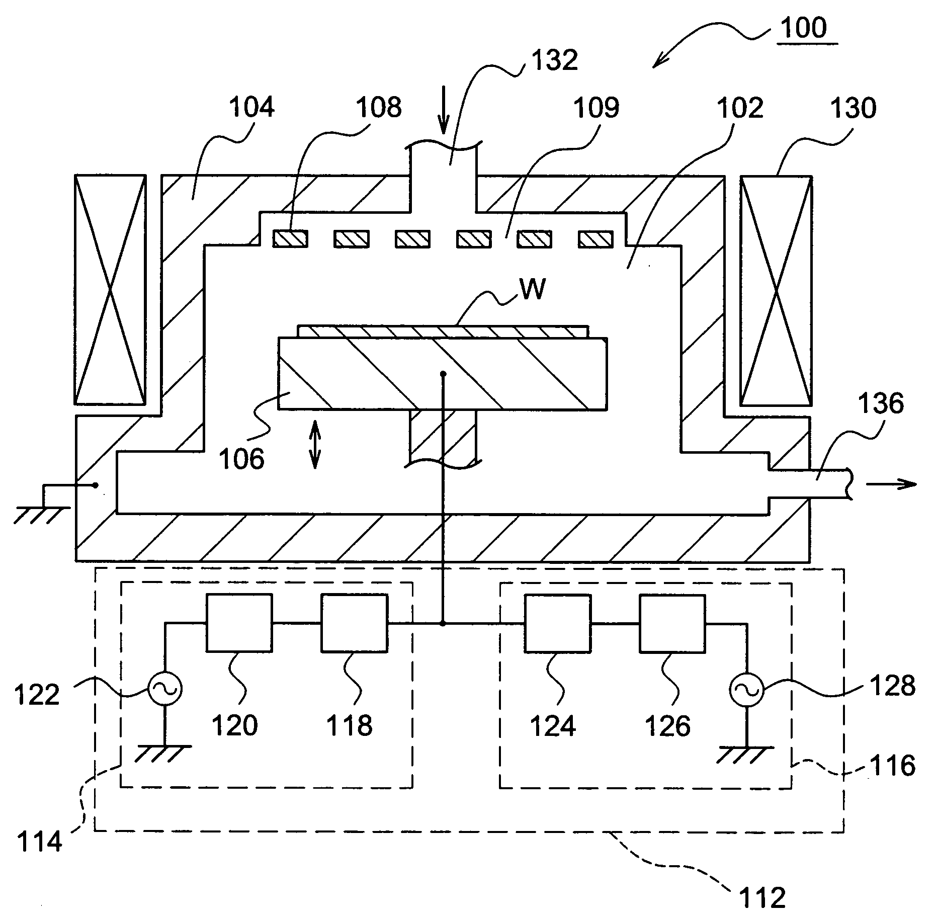
[0070] First of all, the constitution of a plasma etching apparatus according to an embodiment of the invention will be described with reference to the accompanying drawings. FIG. 1 is a schematic sectional view showing the constitution of a plasma etching apparatus 100 according to the first embodiment of the invention.

[0071] As shown in FIG. 1, the plasma etching apparatus 100 has an air tight processing container 104 which is grounded. A processing chamber 102 is formed inside the processing container 104. In the processing chamber 102, a lower electrode 106 capable of concurrently serving as a supporting table for supporting a workpiece such as a semiconductor wafer W mounted thereon, is arranged such that it can move up and down. The lower electrode 106 is kept at a predetermined temperature by means of a temperature adjustment mechanism (not shown), and a heat transfer gas at a predetermined pressure is supplied between the semiconductor wafer W and the lower electrode 106 by...

embodiment 2

[0133] In the next, the second embodiment of the invention will be described with reference to the accompanying drawings. With regard to the first embodiment as descried above, it has been explained assuming that two kinds of high frequency powers are applied to the lower electrode 106 in the plasma etching apparatus 100, at two frequencies of 40 MHz and 3.2 MHz, for example. In the second embodiment, there will be explained about a case where two kinds of high frequency powers are applied to the lower electrode 106 at two frequencies of 100 MHz and 3.2 MHz, for example. Accordingly, a high frequency power source 122 of the plasma etching apparatus 100 according to the second embodiment is constituted such that it can change the high frequency power of 100 MHz.

[0134] Besides, a magnet 130 is constituted such that it can generate a magnetic field around the periphery of a semiconductor wafer W so as to confine the plasma and that the magnetic field strength becomes 10 Gauss or less....


PUM

PropertyMeasurementUnit
self-bias voltageaaaaaaaaaa
frequencyaaaaaaaaaa
frequencyaaaaaaaaaa

Abstract

There is provided an etching method and a plasma etching apparatus capable of taking a large etching selection ratio and of forming a hole having an appropriate shape. When etching an etching target film 204 by using an organic film 202 having a predetermined pattern as a mask, processing gas is introduced into an airtight processing container 104. There are provided a high frequency power source 122 of 40 MHz and a high frequency power source 128 of 3.2 MHz, by which two different kinds of high frequency powers are applied to a lower electrode 106. The power of each high frequency power is properly combined, thereby executing the etching process by using low plasma electron density Ne and high self-bias voltage Vdc which are generated by high frequency power.

Description

TECHNICAL FIELD [0001] The present invention relates to an etching method and a plasma etching apparatus. BACKGROUND TECHNIQUE [0002] At present, in the manufacturing process of semiconductor devices, there is used a technique wherein a predetermined processing of a semiconductor wafer or the like is executed by using plasma formed in an airtight processing container. In this technique using plasma, it becomes one of important subjects how successfully executing the fine and sophisticated processing with high accuracy keeping up with the tendency of high density and high integration in semiconductor device structure. [0003] For example, in an etching process of making a minute structure at a processing target film formed on a semiconductor wafer surface, a processing gas is introduced between a lower electrode capable of serving as a supporting table for supporting the semiconductor wafer placed thereon and an upper electrode facing to the lower one, and a high frequency power is ap...

Claims


Application Information

Patent Timeline
Patent Type & Authority Applications(United States)
IPC IPC(8): H01L21/311
CPCH01J37/32082H01L21/31144H01L21/31116H01J37/32706
Inventor HONDA, MASANOBUNAGASEKI, KAZUYAKIDA, HANAKOYATSUDA, KOICHIITO, YOUBUNINAZAWA, KOICHIROINAZAWA, RIEHAYASHI, HISATAKA
Owner TOKYO ELECTRON LTD
Why Eureka
Try Eureka