

Plasma processing method
a processing method and technology of plasma, applied in the field of plasma processing method, can solve the problems of difficult to obtain the designed shape of etched holes or etched grooves, the surface of the photoresist layer becomes rough during etching, and the need for additional space, so as to improve the etching resistance of an organic layer, reduce the yield, and improve the effect of etching resistan
- Summary
- Abstract
- Description
- Claims
- Application Information
AI Technical Summary
Benefits of technology
Problems solved by technology
Method used
Image

Examples
first embodiment
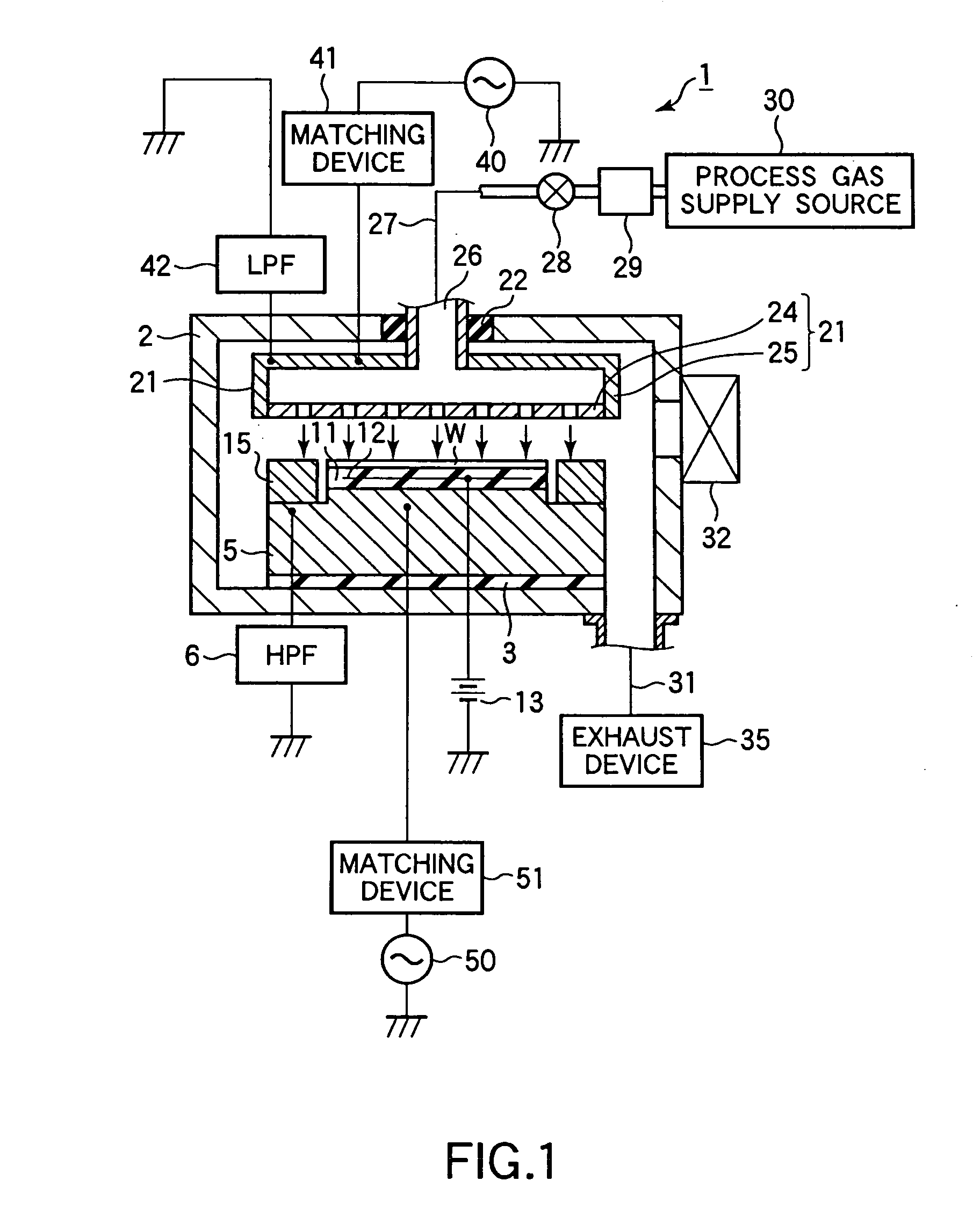
[0082] In this embodiment, the plasma processing apparatus 1 shown in FIG. 1 is used to process a process subject W shown in FIG. 3. This process subject W has an SiO2 film 121 disposed as an etching objective layer, and a photoresist layer 122 of an ArF photoresist or F2 photoresist disposed as a mask layer covering the etching objective layer. This process includes a step of irradiating the process subject W with plasma to improve the plasma resistance of the photoresist layer 122, and a step performed thereafter of plasma-etching the etching objective layer 121 while using the photoresist layer 122 as a mask.
[0083] The ArF photoresist or F2 photoresist may be made of an alicyclic group-containing acrylate resin, cycloolefin resin, cycloolefin-maleic anhydride resin, methacrylate resin, or the like.
[0084] The gate valve 32 is first opened, and the process subject W is transferred into the process container 2 and placed on the electrostatic chuck 11. Then, the gate valve 32 is cl...
second embodiment
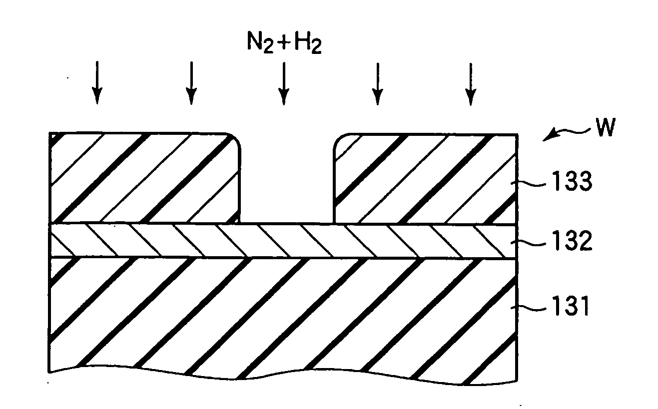
[0095] In this embodiment, the plasma processing apparatus 1 shown in FIG. 1 is used to process a process subject W shown in FIG. 4A. This process subject W has an SiO2 film 131, an antireflective film 132 covering the SiO2 film 131, and a photoresist layer 133 of an ArF photoresist or F2 photoresist covering the antireflective film 132. This process includes a first etching step (FIG. 4A) of etching the antireflective film 132 through a pattern opening of the photoresist layer 133 and improving the plasma resistance of the photoresist layer 133, and a second etching step (FIG. 4B) performed thereafter of plasma-etching the SiO2 film 131 through the photoresist layer 133.
[0096] A process subject W is first transferred into and placed in the process container 2. A process gas used also as a first etching gas, such as N2 and H2, is supplied from the process gas supply source 30, and the pressure in the process container 2 is set at a predetermined value, such as 107 Pa (800 mTorr). A...
third embodiment
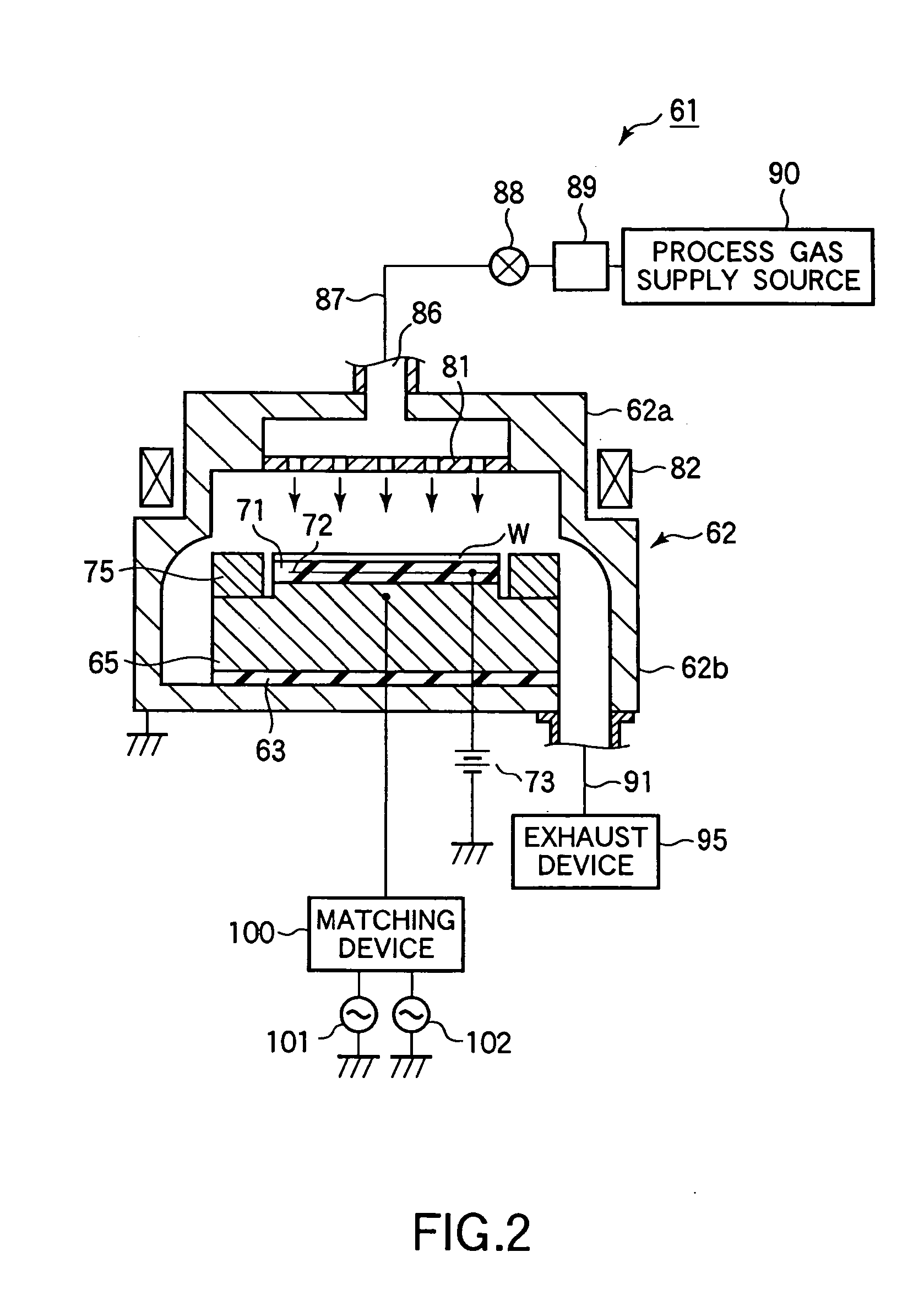
[0105] In this embodiment, the plasma processing apparatus 61 shown in FIG. 2 is used to process a process subject W shown in FIG. 5A. This process subject W has an SiO2 film 141 disposed as an etching objective layer, an antireflective film 142 covering the SiO2 film 141, and a photoresist layer 143 of an ArF photoresist or F2 photoresist covering the antireflective film 142. This process includes a step (FIG. 5A) of using plasma to improve the plasma resistance of the photoresist layer 143 and etch the antireflective film 142 through an opening pattern 143a of the photoresist layer 143, and a step (FIG. 5B) performed thereafter of plasma-etching the SiO2 film 141 through the photoresist layer 143.
[0106] Also in this embodiment, the ArF photoresist or F2 photoresist may be made of an alicyclic group-containing acrylate resin, cycloolefin resin, or cycloolefin-maleic anhydride resin. As the antireflective layer, an organic polymeric material or amorphous carbon may be used.
[0107] ...
PUM
| Property | Measurement | Unit |
|---|---|---|
| Pressure | aaaaa | aaaaa |
| Pressure | aaaaa | aaaaa |
| Pressure | aaaaa | aaaaa |
Abstract
Description
Claims
Application Information