Method for forming nanostructured carbons, nanostructured carbons and a substrate having nanostructured carbons formed thereby

a technology of nanostructured carbons and nanostructured carbons, which is applied in the field can solve the problems of increasing equipment expenses and production costs, complex equipment, and difficult to make nanostructured carbons directly grown on a planar substrate, and achieves the effect of forming nanostructured carbons easily and quickly

Inactive Publication Date: 2005-05-19
KONICA MINOLTA INC
View PDF2 Cites 61 Cited by
  • Summary
  • Abstract
  • Description
  • Claims
  • Application Information

AI Technical Summary

Benefits of technology

[0010] This invention has been made taking the above circumstances into consideration. The first object of this invention is to provide a method for forming nanostructured carbons easily and quickly. Its second object is to provide a method for forming nanostructured carbons on various kinds of substrates.

Problems solved by technology

This makes the equipment complicated and increases the equipment expenses and production costs.
Further, the arc-discharge process is hard to make nanostructured carbons directly grown on a planar substrate.
The processes can directly form nanostructured carbons only locally but cannot form them directly on a wide substrate at all.
Therefore, the substrates on which nanostructured carbons are to be directly formed must be very heat resistant and they are limited to ceramics and quartz glass.
Naturally, this process is not applicable to substrates of ordinary glasses such as soda glasses and low alkali glasses (including non-alkali glasses) and plastic substrates.

Method used


Image

  • Method for forming nanostructured carbons, nanostructured carbons and a substrate having nanostructured carbons formed thereby
  • Method for forming nanostructured carbons, nanostructured carbons and a substrate having nanostructured carbons formed thereby
  • Method for forming nanostructured carbons, nanostructured carbons and a substrate having nanostructured carbons formed thereby

Examples


example 1

[0107] (Process of Attaching Fine Metal Particles to Substrate Surfaces)

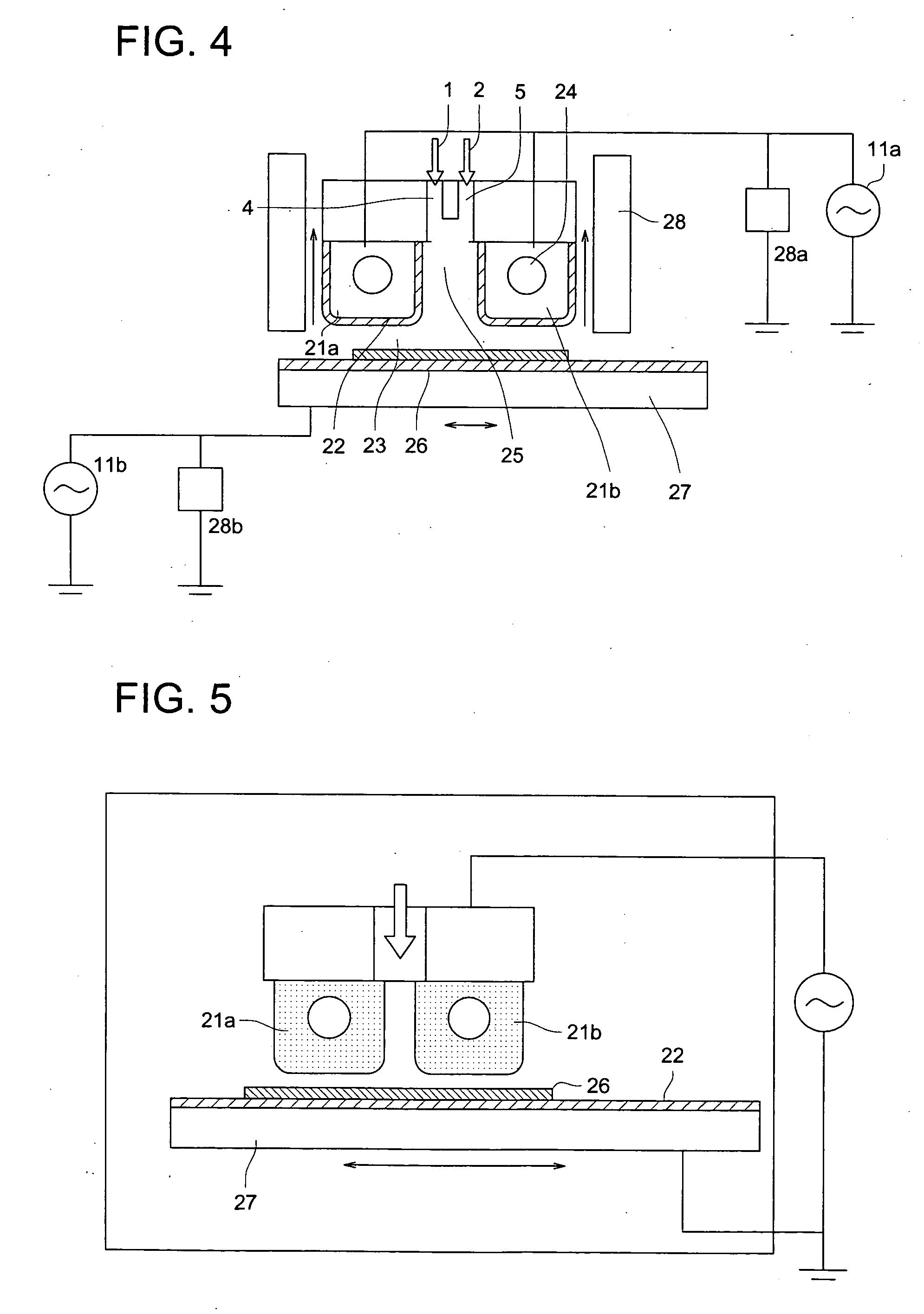
[0108] We attached fine metal particles to substrate surfaces by using equipment having a configuration of FIG. 5.

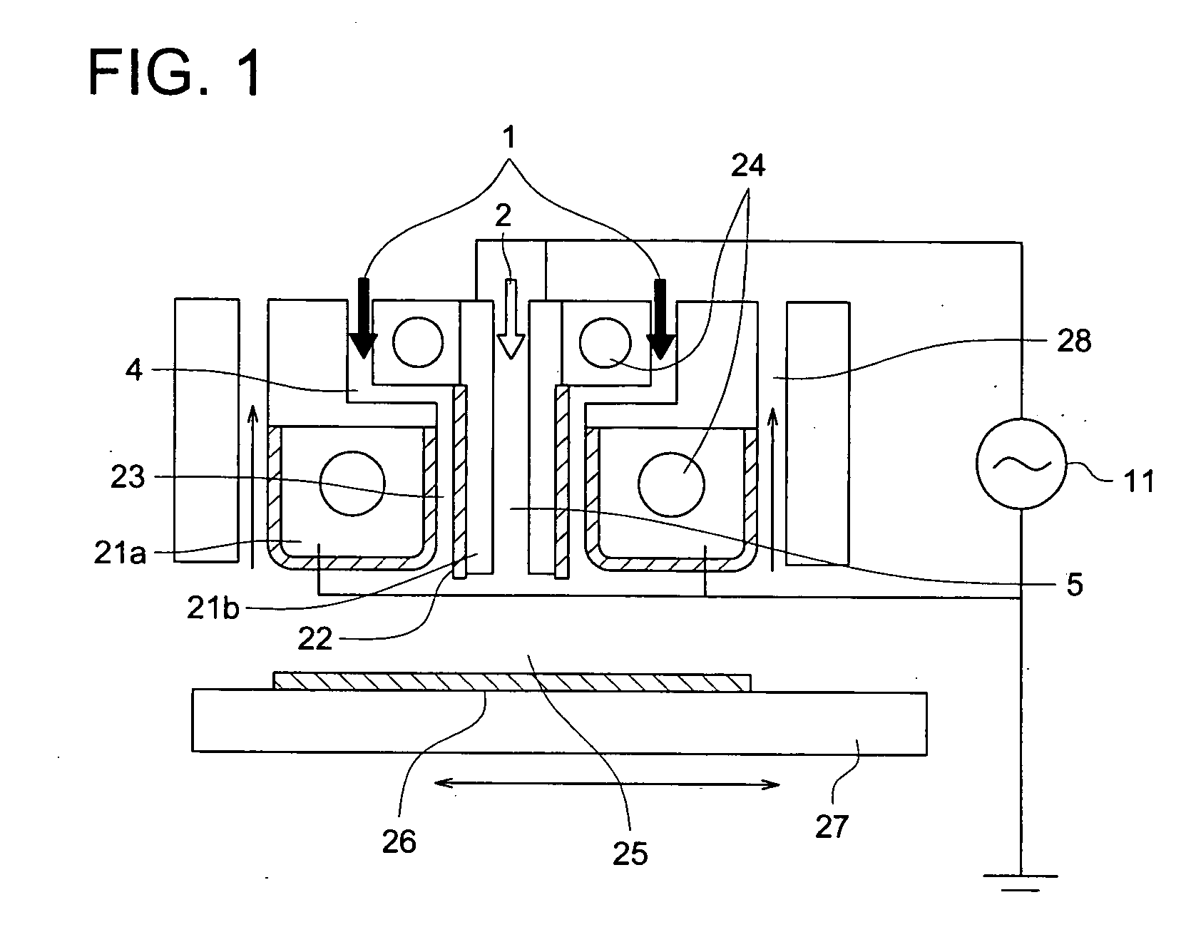
[0109] We prepared pure-iron (Fe) targets of 20 mm×20 mm×120 mm (long) as the electrodes 21a and 21b. Each target had its edges rounded (R3) and contained a through-hole through which silicone oil flowed to control the electrode temperature by heat exchange.

[0110] The moving stage electrode 27 was made of a titanium plate (JIS Class 2 titanium) of 100 mm×500 mm×20 mm and had three through-holes to control the electrode temperature. The surface of this electrode was coated with alumina ceramic by thermal spraying to have a ceramic coat of 0.8 mm thick. Then a dielectric layer 22 was formed on the alumina ceramic layer of the stage electrode by applying an organic solution of alkoxysilane monomer to the alumina ceramic layer, drying thereof, and sealing thereof at 300° C.

[0111] We arranged two of t...

example 2

[0122] (Example of using a Substrate having a Conductive Layer on it)

[0123] The metal particle attaching process and the nanostructured carbon fabricating process of this example are the same as those of Example 1 but Example 2 uses a substrate having a conductive layer on it. Example 2 could also get carbon materials of carbon nanotubes almost similar to those obtained by Example 1. A conductive layer was formed on the substrate as follows:

[0124] We placed a base material on the moving stage electrode 27 in the equipment of FIG. 5 (having electrodes coated with dielectric material) and purged the gas in the container with nitrogen gas until the concentration of oxygen gas in the container becomes 50 ppm.

[0125] We fed a mixture gas of 95.9% by volume of nitrogen gas, 0.1% by volume of aluminum acetyl acetate vapor, and 4% by volume of hydrogen gas into the equipment and applied a high frequency voltage of 50 kHz, 8 KV to one of the electrodes and a high frequency voltage of 13.56...

example 3

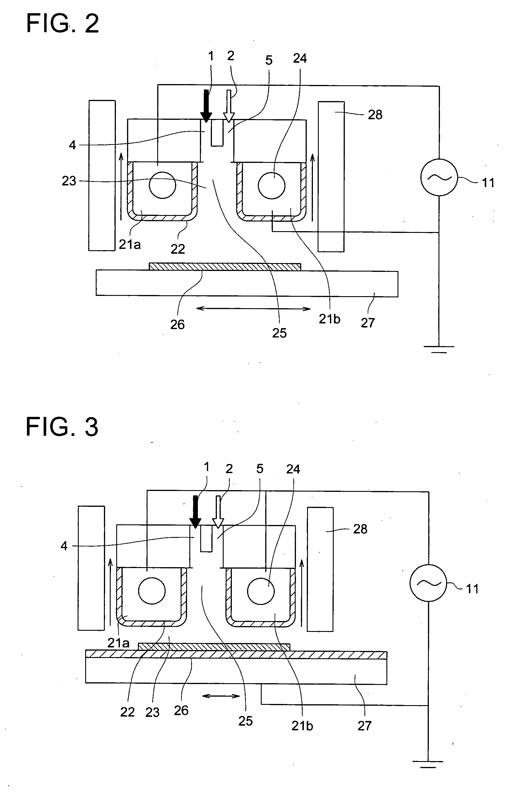
[0130] We formed nanostructured carbons on a substrate having a conductive layer on it in the manner similar to Example 1 by using the equipment configuration of FIG. 4.

[0131] We prepared, as electrodes 21a and 21b, titanium bars (JIS Class 2 titanium) of 20 mm×20 mm×120 mm (long). Each electrode bar had its edges rounded (R3) and contained a through-hole for heat exchange. The surface of each electrode bar was coated with alumina ceramic by thermal spraying to have a ceramic coat of 0.8 mm thick. Then a dielectric layer 22 was formed on the alumina ceramic layer of each electrode bar by applying an organic solution of alkoxysilane monomer to the alumina ceramic layer, drying thereof, and sealing thereof at 300° C.

[0132] We arranged two of the above electrode bars to form a clearance of 2 mm wide between them so that the raw material gas containing the discharge gas might flow through this clearance. We used the same moving stage electrode 27 as what was prepared for the metal par...


PUM

PropertyMeasurementUnit
frequencyaaaaaaaaaa
temperatureaaaaaaaaaa
atmospheric pressureaaaaaaaaaa

Abstract

A method for forming nanostructured carbons comprising the steps of: generating a plasma by supplying at least a discharge gas between opposing electrodes and applying a high-frequency voltage between the electrodes under an approximately atmospheric pressure; existing a material gas for forming the nanostructured carbons with the plasma to generate an activated material gas; and exposing a substrate to the activated material gas.

Description

RELATED APPLICATION [0001] This application is based on patent applications Nos. 2003-386296, 2003-416030 and 2004-109735 filed in Japan, the entire content of which is hereby incorporated by reference. BACKGROUND [0002] 1. Field of the invention [0003] This invention relates to a method of forming nanostructured carbons and particularly, a method of forming said materials easily and quickly. [0004] 2. Description of the Related Art [0005] Recently, a lot of researches and studies have been made on nanostructured carbons on the order of a few nanometers (nm) in diameter such as carbon nanotubes, carbon nanofibers, and graphite nanofibers. A carbon nanotube is a seamless tube made by wrapping a single planar sheet (called a graphene sheet) of 6-carbon rings. A single wall nanotube is made of a single graphene sheet. A multi-wall nanotube is made of a plurality of graphene sheets wrapped in a nested structure. Graphite nanofibers are composed of cylindrically laminated graphene sheets...

Claims


Application Information

Patent Timeline
Patent Type & Authority Applications(United States)
IPC IPC(8): C01B31/02D01F9/12H05H1/24
CPCB82Y10/00B82Y30/00B82Y40/00C01B31/022H05H1/24C01B2202/02D01F9/12H01J2201/30469C01B31/0233H05H2240/10C01B32/158C01B32/162C01B32/159H05H2245/50C01B32/16B01J19/12H05H1/2406
Inventor KONDO, YOSHIKAZU
Owner KONICA MINOLTA INC
Why Eureka
Try Eureka