
Magnetic memory device

Inactive Publication Date: 2005-06-02
SONY CORP
View PDF3 Cites 30 Cited by
  • Summary
  • Abstract
  • Description
  • Claims
  • Application Information

AI Technical Summary

Benefits of technology

[0033] On the basis of such recognition described above, the inventors of the present invention have discovered that by placing the memory elements avoiding the edge portion and the center portion of the magnetic shield layer, that is, by placing the memory elements in a region between the center portion of the magnetic shield layer, in which magnetic saturation easily tends to occur thereby allowing for an internal leakage magnetic field strength to become large, and the edge portion of the magnetic shield layer, in which no magnetic shield effect exists because of a direct exposure to an external magnetic field, the memory elements are ensured to operate normally without being affected by the internal leakage magnetic field, thereby enabling successfully to achieve the magnetic memory device according to the present invention.

Problems solved by technology

However, the flash memory has a drawback that a write speed is low in the order of ″ seconds.
On the other hand, also in the FRAM, problems are cited that because the number of rewritable frequencies is 1012 to 1014, the endurance thereof is too small to completely replace SRAM (Static Random Access Memory) or DRAM (Dynamic Random Access Memory), and that micro fabrication of a ferroelectric capacitor is not easy.
As described above, although the MRAM is expected as a high speed and large capacity non-volatile memory, because of use of the magnetic material for retention of information, there is such a problem that information is erased or rewritten by the effect of an external magnetic field.
In addition, because a coercive force (Hc) when writing is in a range of approximately a few Oe to 10 Oe, if an internal leakage magnetic field greater than that resulting from an external magnetic field is applied, it sometimes becomes impossible selectively to write to a designated memory cell.
However, when the passivation film of the element is formed from ferrite as disclosed in U.S. Pat. No. 5,902,690, because of a low magnetic saturation in the ferrite itself (for example, 0.2 to 0.5 tesla (T) in general ferrite materials), it is impossible completely to prevent penetration of external magnetic fields.
Further, although a film thickness is not described in U.S. Pat. No. 5,902,690, because a thickness of a normal passivation film is about 0.1 ″m or so at most, it is too thin to serve as a magnetic shield layer, thereby any substantial effect cannot be expected.
Moreover, in the case if ferrite is to be used as the passivation film, because the ferrite is an oxide magnetic material, when it is deposited by sputtering, an oxygen defect tends to occur, thereby making it difficult to obtain a perfect ferrite to be used as the passivation film.
However, although the permeability of the Mu metal disclosed in U.S. Pat. No. 5,939,772 is very high to become ″i=100,000 or so, the magnetic saturation thereof is very low to be 0.7 to 0.8 T, at which it will easily saturate to an external magnetic field consequently to become ″=1, therefore, there is a problem that in order to obtain a perfect magnetic shielding effect, a thickness of the shield layer must be increased considerably large.
Therefore, as the structure for enabling to prevent penetration of magnetic fields of several hundreds Oe, in practice, it is not yet perfect as the magnetic shield layer in view of both drawbacks that the saturation magnetization thereof is too small and that the thickness thereof is too thin.
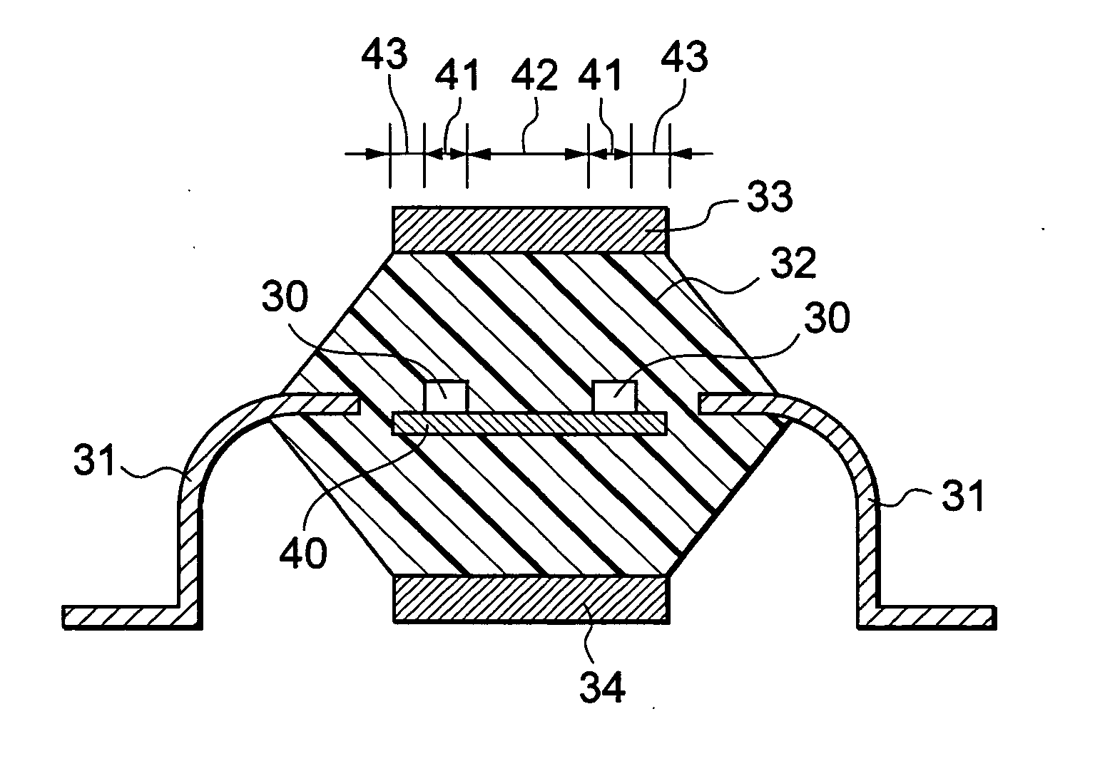
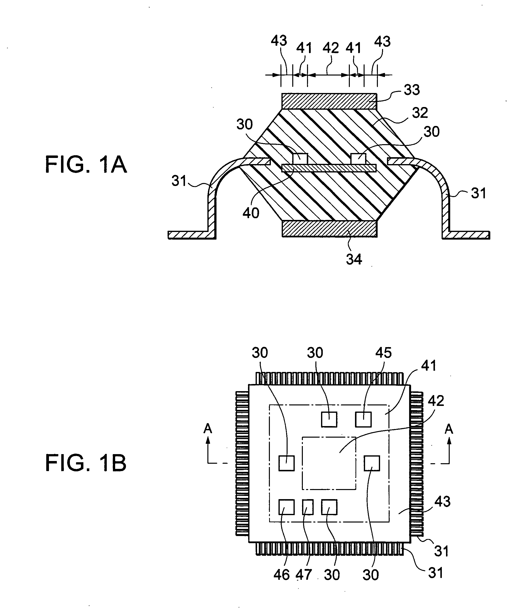
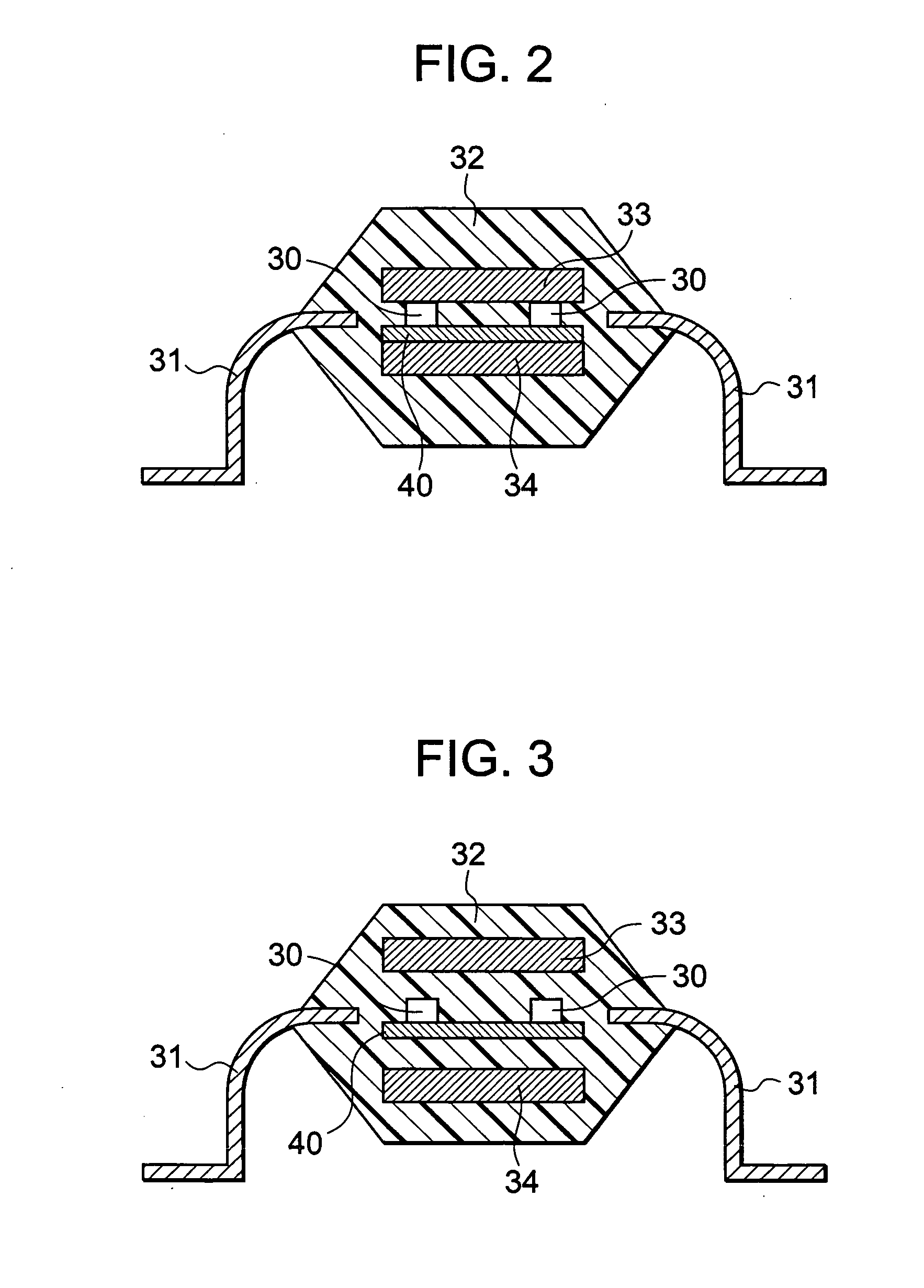
Still further, in Japanese Patent Application Publication No. 2001-250206, although a magnetic shield structure using soft iron or the like is disclosed, as this covers only the upper portion of the element, it is not perfect as the magnetic shield.
Also, the magnetic characteristics thereof are not sufficient because that the saturation magnetization of the soft iron is 1.7 T and the permeability thereof is ″i=300 or so.
Therefore, even if a magnetic shield is fabricated using the structure disclosed in Japanese Patent Application Publication JP-A Laid-Open No. 2001-250206, it would be very difficult to completely prevent the penetration of external magnetic fields.

Method used


Image

  • Magnetic memory device
  • Magnetic memory device
  • Magnetic memory device

Examples


Embodiment Construction

[0053] In a magnetic memory according to the preferred embodiment of the invention, when a length from one side of a magnetic shield layer to an opposed side thereof is assumed to be L, it is desirable for memory elements to be disposed in a region between a position at 0.1 L inward from the above-mentioned one side and a position at 0.15 L outward from the center of the magnetic shield layer toward the above-mentioned one side thereof, in consideration that an adverse effect by an internal leakage magnetic field can be easily avoided by the arrangement described above.

[0054] In this case, assuming that the magnetic shield layer is provided on both sides (top and bottom) of the memory element respectively, and that a distance between these magnetic shield layers, a length from the aforementioned one side of the magnetic shield layer to the opposed side thereof, and an external magnetic field to be applied are constant respectively, it is desirable for the aforementioned memory elem...


PUM


Abstract

A memory device is proposed which enables to guarantee the operation of MRAM elements being magnetically shielded against a large external magnetic fields without being affected by an internal leakage magnetic field. The MRAM elements 30 which are shielded by magnetic shield layers 33, 34 are placed at an intermediate region 41 avoiding an edge region 43 and a center region 42 of the magnetic shield layers 33, 34 so that the MRAM element is secured to operate normally without being affected by the internal leakage magnetic field avoiding the edge region 43 where the magnetic shield effect is reduced by the exterior magnetic field, and avoiding the central region 42 where the internal leakage magnetic field is large

Description

TECHNICAL FIELD [0001] The present invention relates to a magnetic memory device constructed as a magnetic random access memory (MRAM) or a so-called non-volatile MRAM (Magnetic Random Access Memory) which is comprised of memory elements made by laminating a magnetization pinned layer in which the orientation of magnetization is fixed and a magnetic layer in which the orientation of magnetization is changeable, or to any magnetic memory device comprising memory elements having a magnetic layer capable of being magnetized. BACKGROUND ART [0002] With a rapid prevalence of information communication equipment, in particular, of personal compact equipment such as portable terminals, a further improvement in performance inclusive of larger scale integration, faster speed, lower power consumption or the like is demanded for their elements such as memories, logics and the like. [0003] In particular, the non-volatile memory is considered to be indispensable in the age of ubiquitous. If a pow...

Claims


Application Information

Patent Timeline
IPC IPC(8): H01L21/8246H01L23/00H01L23/552H01L27/105H01L27/22H01L43/08
CPCB82Y10/00H01L23/552H01L27/222H01L2224/16H01L2924/01004H01L2924/01025H01L2924/01077H01L2924/1305H01L2924/01078H01L2924/01079H01L2924/3025H01L2924/01019H01L2924/00H10B61/00G11C11/15H10B99/00
Inventor KATO, YOSHIHIROOKAYAMA, KATSUMIKOBAYASHI, KAORUYAMAMOTO, TETSUYAIKARASHI, MINORU
Owner SONY CORP
Features
  • Generate Ideas
  • Intellectual Property
  • Life Sciences
  • Materials
  • Tech Scout
  • Unparalleled Data Quality
  • Higher Quality Content
  • 60% Fewer Hallucinations
Learn More