Ultra-thin Si channel MOSFET using a self-aligned oxygen implant and damascene technique

a technology of oxygen implants and damascene, which is applied in the direction of semiconductor devices, electrical equipment, transistors, etc., can solve the problems of series resistance increase, degrade manufacturing yield, circuit performance degradation, etc., and achieves lateral spread, slow circuit performance, and parasitic capacitance increase

Active Publication Date: 2005-06-02
GLOBALFOUNDRIES US INC
View PDF6 Cites 72 Cited by
  • Summary
  • Abstract
  • Description
  • Claims
  • Application Information

AI Technical Summary

Benefits of technology

[0006] In some prior art thin Si-channel devices, source / drain extension regions are implanted prior to raised source / drain formation resulting in a number of disadvantageous effects. For example, p-type extension regions require a thick offset spacer to control dopant diffusion and disadvantageously result in a high resistance region formed underlying the thick offset spacer. Additionally, in some prior art thin channel devices, the extension implants are conducted prior to raised source / drain formation; therefore subjecting the extension implant dopants to the significant thermal budget of the raised source / drain process, which may result in unwanted dopant diffusion. Further, the incubation time is different for p-type and n-type doped Si leading to substantially different raised source / drain thickness for p-type and n-type doped regions.
[0007] In one prior art thin Si channel device, a wide disposable spacer is utilized to grow the raised source / drain regions. High-energy implants are then performed to form deep source / drain regions. Following the high-energy implant, the wide disposable spacer is removed and extension regions are implanted. This prior art process overcomes excessive extension dopant diffusion and the epitaxial Si growth rate differential between p-type and n-type regions, but does not overcome the formation of high resistance regions outside the raised source / drain area, which are key to the performance of thin SOI MOSFETs. The formation of high resistance regions outside the raised source / drain area is also cost ineffective. In addition, the raised source drain regions cause increased parasitic capacitance, which slows down circuit performance.
[0008] Another prior art scheme utilizes a dummy structure as an implant mask for implanting oxygen ions into a bulk Si substrate. This process simultaneously creates a buried oxide layer and also forms a thin Si region; the thin Si region is produced by the dummy structure. However, in order to create a suitably thick buried oxide layer, a high-energy oxygen implant is needed. The large energy distribution of the high-energy implant required to form a suitably thick buried oxide layer disadvantageously results in a substantially wide region of thin Si that is much larger, in a lateral direction, than the desired width of the channel region. The lateral spread of the oxygen implant is proportional to the implant depth. Specifically, the lateral spread for oxygen implants conducted through gate structures into substrates utilized in conventional semiconducting devices is equal to ⅓ the depth of the oxygen implant in the vertical direction. The lateral spread is also affected by the implant energy, where the greater the implant energy the greater the lateral spread.
[0009] Referring to FIG. 1, when using the prior art method in order to produce a low junction capacitance SOI device in a bulk Si substrate 37, a buried oxide layer 36 having a vertical thickness T5 on the order of 200.0 nm must be formed as well as an SOI layer 35 having a thickness T2 on the order of about 70 nm. Taking into account the vertical spread of oxygen dopant, in order to form a thinned channel region 26 underlying the dummy gate region 18, while simultaneously forming a suitable buried oxide region 36, the oxygen implant peak must extend through the dummy gate 18 (T4=70.0 nm); through the desired thickness of the thin channel 26 (T1=20.0 nm) and extend to a depth equal to half the thickness of the desired buried oxide 36 thickness (T3=½(200.0 nm)). In the present example, the required peak implant depth to produce a suitable buried oxide layer 36 is equal to: 20.0 nm+70.0 nm+½(200.0 nm)=190.0 nm
[0010] As stated previously, the lateral spread of oxygen dopant W1 is equivalent to ⅓ the depth (vertical thickness) of the peak oxygen implant. Therefore, in the present example of the prior art the lateral spread of the oxygen dopant is on the order of about 60.0 nm. The lateral spread results in a channel region 26 that is not aligned with the edges of the overlying gate region 18, therefore producing thin silicon high resistance regions 40 at the terminal ends of the channel region 26 of the device. Additionally, the high-energy implant can produce defects and high levels of metallic contamination.
[0011] In view of the state of the art mentioned above, it would be highly desirable to provide a thin channel silicon-on-insulator device that overcomes the above-described disadvantages. More specifically, it would be highly desirable to provide thin channel silicon-on-insulator devices having low external resistance without raised source / drain regions. It would also be advantageous to provide an ultra-thin channel device with lower parasitic capacitance. SUMMARY OF THE INVENTION

Problems solved by technology

A disadvantage of thin channel devices is that as the silicon-on-insulator (SOI) film is thinned the series resistance increases.
Raised source / drain regions typically degrade manufacturing yield and also increase parasitic capacitance, which causes degradation in circuit performance.
In some prior art thin Si-channel devices, source / drain extension regions are implanted prior to raised source / drain formation resulting in a number of disadvantageous effects.
For example, p-type extension regions require a thick offset spacer to control dopant diffusion and disadvantageously result in a high resistance region formed underlying the thick offset spacer.
Additionally, in some prior art thin channel devices, the extension implants are conducted prior to raised source / drain formation; therefore subjecting the extension implant dopants to the significant thermal budget of the raised source / drain process, which may result in unwanted dopant diffusion.
This prior art process overcomes excessive extension dopant diffusion and the epitaxial Si growth rate differential between p-type and n-type regions, but does not overcome the formation of high resistance regions outside the raised source / drain area, which are key to the performance of thin SOI MOSFETs.
The formation of high resistance regions outside the raised source / drain area is also cost ineffective.
In addition, the raised source drain regions cause increased parasitic capacitance, which slows down circuit performance.
The large energy distribution of the high-energy implant required to form a suitably thick buried oxide layer disadvantageously results in a substantially wide region of thin Si that is much larger, in a lateral direction, than the desired width of the channel region.
Additionally, the high-energy implant can produce defects and high levels of metallic contamination.

Method used


Image

  • Ultra-thin Si channel MOSFET using a self-aligned oxygen implant and damascene technique
  • Ultra-thin Si channel MOSFET using a self-aligned oxygen implant and damascene technique
  • Ultra-thin Si channel MOSFET using a self-aligned oxygen implant and damascene technique

Examples


Embodiment Construction

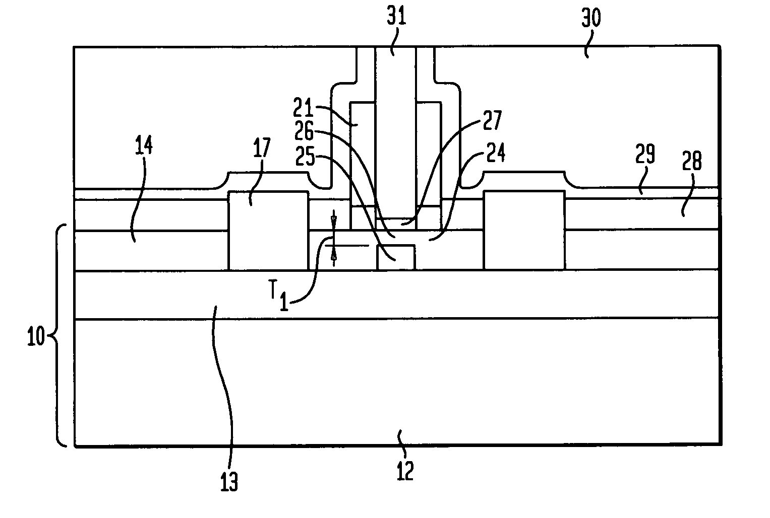
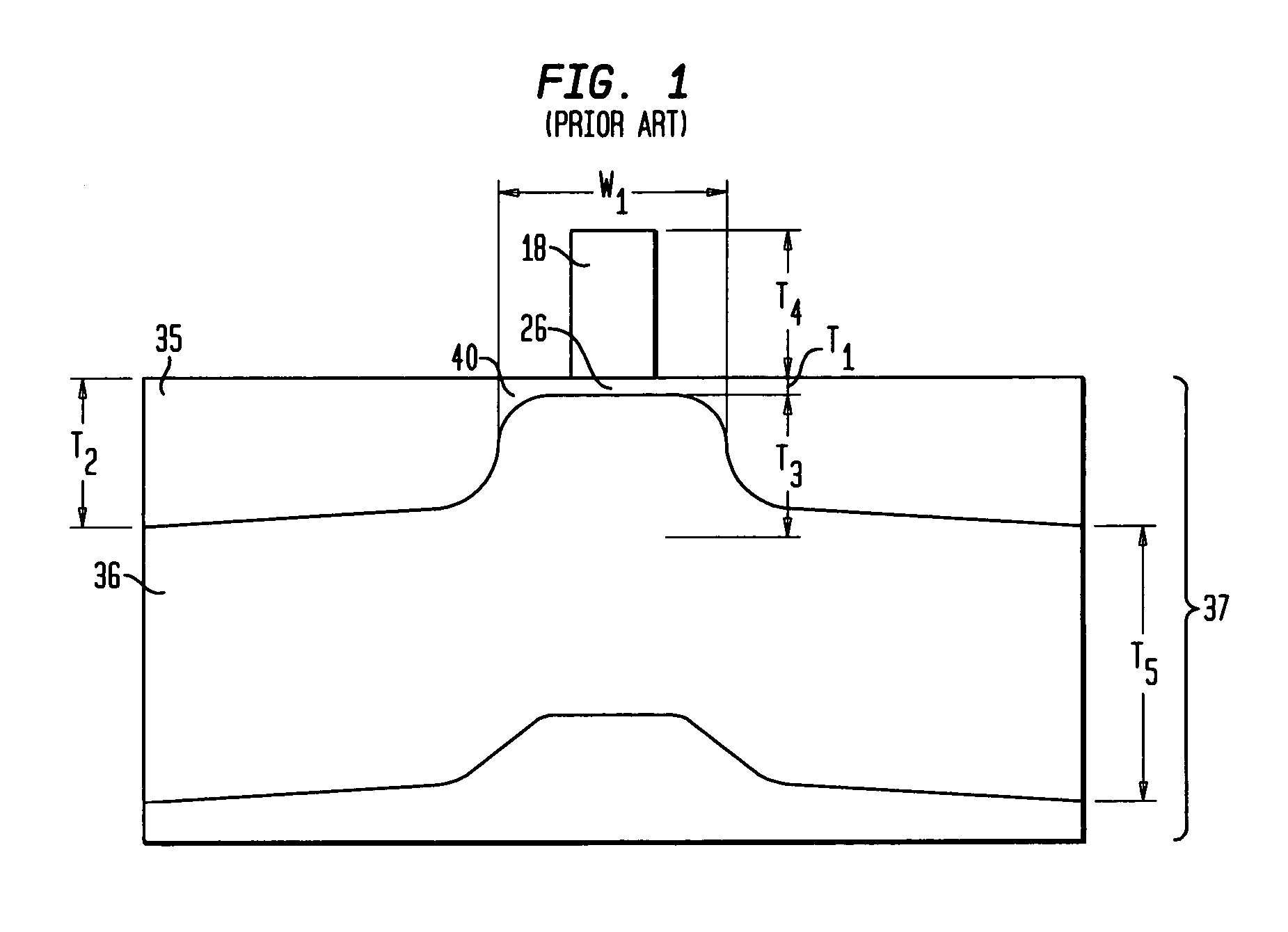
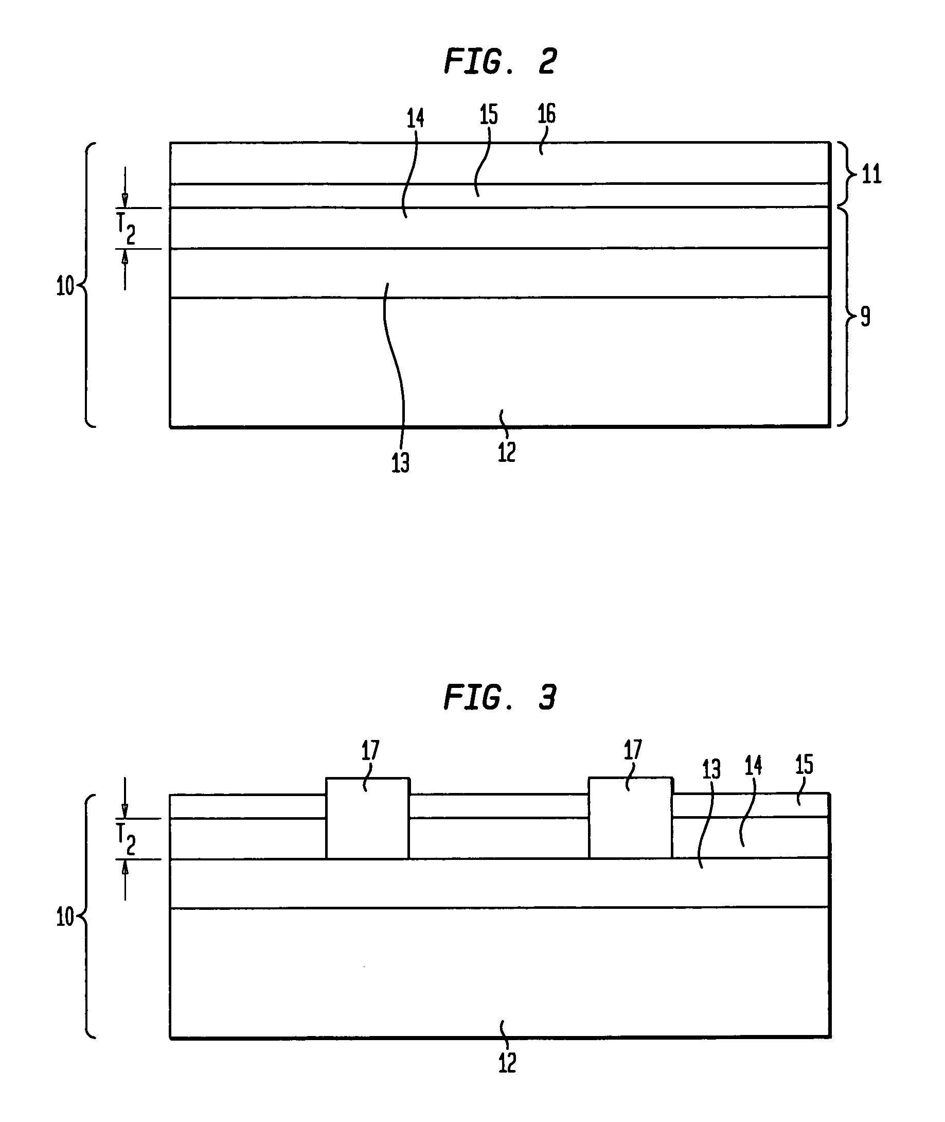
[0039] The present invention provides a thin channel SOI MOSFET having low resistance source / drain regions 24 formed in the SOI layer 14 of a silicon-on-insulator (SOI) substrate 9. The thickness T1 of the thin channel region 26 of the present invention is on the order of less than about 50.0 nm, preferably ranging from approximately 3.0 nm to approximately 30.0 nm.

[0040] The inventive thin channel MOSFET further comprises a localized oxide region 25 self-aligned to an overlying gate region, where the localized oxide region 25 in conjunction with the buried insulating layer 13 of the SOI substrate 9 effectively thin the device channel 26 while allowing for the formation of source / drain extensions 24 having a thickness equal to the thickness of the SOI layer 14 of the substrate. The present invention also provides a method for forming thin channel SOI devices where a dummy gate region 23 in conjunction with an oxygen implant 40 form the localized oxide region 25 that effectively thi...


PUM


Abstract

The present invention provides a thin channel MOSFET having low external resistance. In broad terms, a silicon-on-insulator structure comprising a SOI layer located atop a buried insulating layer, said SOI layer having a channel region which is thinned by the presence of an underlying localized oxide region that is located on top of and in contact with said buried insulating layer; and a gate region located atop said SOI layer, wherein said localized oxide region is self-aligned with the gate region. A method for forming the inventive MOSFET is also provided comprising forming a dummy gate region atop a substrate; implanting oxide forming dopant through said dummy gate to create a localized oxide region in a portion of the substrate aligned to the dummy gate region that thins a channel region; forming source / drain extension regions abutting said channel region; and replacing the dummy gate with a gate conductor.

Description

FIELD OF THE INVENTION [0001] The present invention relates to semiconductor devices and methods of manufacture, and more particularly to a method for manufacturing an improved metal oxide semiconductor (MOS) transistor having an ultra-thin channel (on the order of about 50 nm or less). BACKGROUND OF THE INVENTION [0002] Field effect transistors (FETs) are the basic building block of today's integrated circuits (ICs). Such transistors can be formed in conventional bulk semiconductor substrates (such as silicon) or in the SOI layer of a silicon-on-insulator (SOI) substrate. [0003] In order to be able to make ICs, such as memory, logic, and other devices, of higher integration density than currently feasible, one has to find ways to further downscale the dimensions of field effect transistors (FETs), such as metal-oxide-semiconductor field effect transistors (MOSFETs) and complementary metal oxide semiconductors (CMOS). Scaling achieves compactness and improves operating performance i...

Claims


Application Information

Patent Timeline
Patent Type & Authority Applications(United States)
IPC IPC(8): H01L21/336H01L29/786
CPCH01L29/66545H01L29/66772H01L29/78696H01L29/78684H01L29/78609
Inventor BOYD, DIANE C.DORIS, BRUCE B.IEONG, MEIKEISADANA, DEVENDRA K.
Owner GLOBALFOUNDRIES US INC
Why Eureka
Try Eureka