Antenna and communication device

Inactive Publication Date: 2005-06-02
FUJIFILM BUSINESS INNOVATION CORP
View PDF6 Cites 32 Cited by
  • Summary
  • Abstract
  • Description
  • Claims
  • Application Information

AI Technical Summary

Benefits of technology

[0017] It is preferable that the carbon nanotube is a multi-wall carbon nanotube. When the radiating portion of the antenna is structured by the multi-wall carbon nanotube, it becomes easy to handle, and the manufacture efficiency

Problems solved by technology

However, even in both the cases of the fixed helical antenna and of the planar inverted-F antenna, the communication band of the antenna element is specified and therefore it is impossible to maintain the efficiency ove

Method used


Image

  • Antenna and communication device
  • Antenna and communication device
  • Antenna and communication device

Examples


Example

First Example

(Fabrication of Antenna)

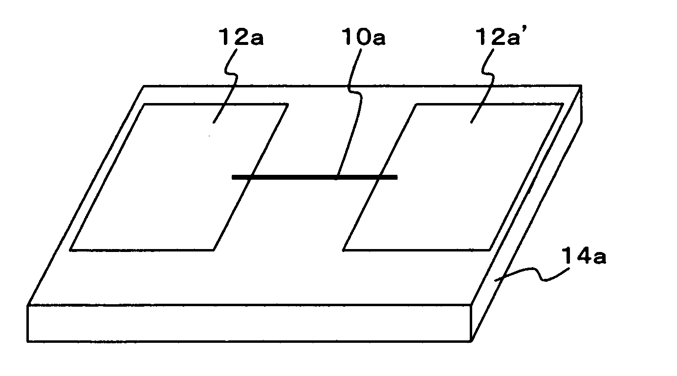
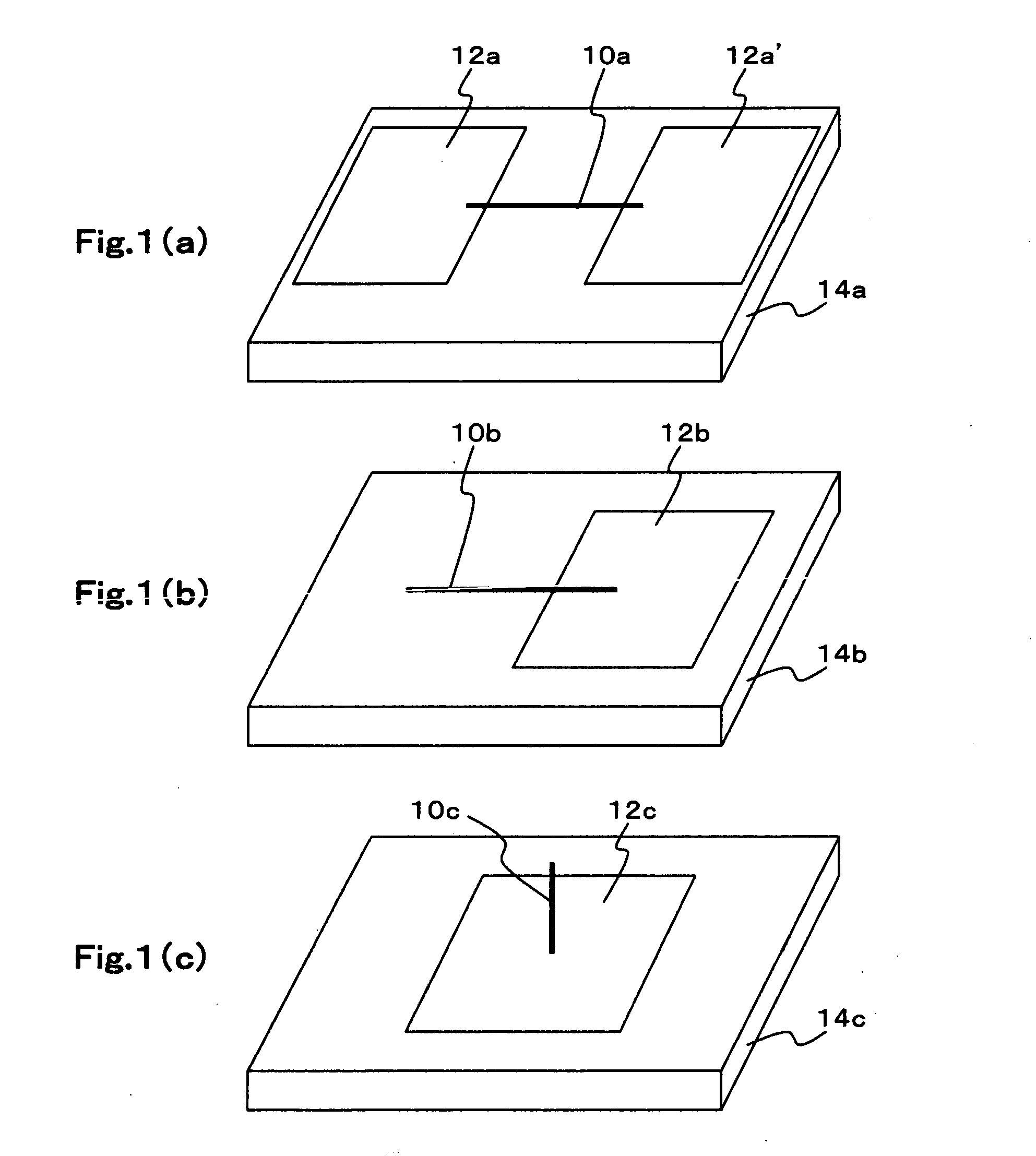
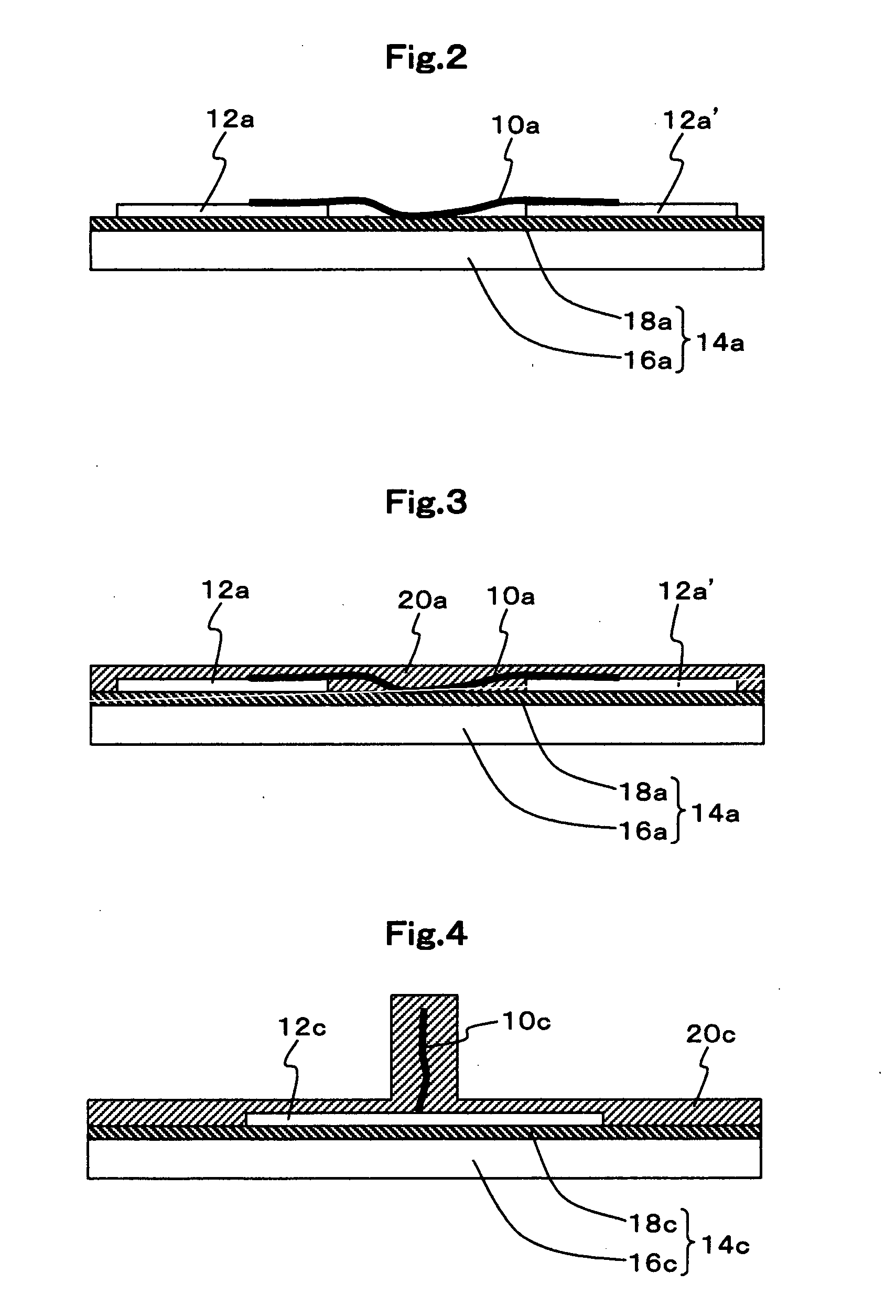
[0108] First, a pair of electrodes for connecting a multi-wall carbon nanotube were formed on an SiO2 layer side surface of an SiO2 / Si substrate (the thickness of an Si substrate as a support plate was 500 μm, and the thickness of an SiO2 layer as a dielectric layer was 500 nm) so as to adjust a gap between those two electrodes to 2.5 μm. A mask deposition method was used as the forming method, and an electrode material as used was Au / Cr. The thickness of the electrodes was set to 50 nm.

[0109] One multi-wall carbon nanotube (40 nm in diameter and 4 μm in length) fabricated through the in-magnetic-field arc electric discharge process was so arranged as to bridge the gap between the pair of electrodes thus obtained, and fixed. More specifically, a micromanipulator was introduced in an scanning electron microscope (SEM). The detailed procedure will be described below.

[0110] First, a cathode deposit containing a high-purity multi-wall carbon nan...

Example

Second Example

(Fabrication of Antenna)

[0115] A pair of Au / Cr electrodes were fabricated on an SiO2 layer side surface of the SiO2 / Si substrate with a gap of 10 μm therebetween as in the first example. The thickness of the electrodes was 50 nm.

[0116] The single-wall carbon nanotube composed through the arc electric discharge method was purified (about 1 nm in the mean diameter), and dispersed in dimethylformamide at the ratio of 10 g / l. One droplet of the single-wall carbon nanotube was dropped in the gap between the pair of electrodes by using a micropipette and was then naturally dried.

[0117] The antenna of this example was fabricated in the above-manner. FIG. 11 is an SEM photographic image (magnification of 3000 times) obtained by extracting only a portion at which a carbon nanotube is located and enlarging the extracted portion in the antenna in accordance with this example of the present invention. In FIG. 11, the single-wall carbon nanotubes seem to be white thin lines, a...

Example

First Comparative Example

[0120] As a comparative measurement, an antenna made of high orientation graphite was used as the antenna of a first comparative example. The antenna has been conventionally used as the antenna of the general communication device. The high-orientation graphite has graphite oriented in a C-axial direction, and its size is 10 mm in length, 10 mm in width and 2 mm in thickness.

[0121] In the antenna according to the first comparative example, the electromotive force was measured in the same manner as that in the first example. The electromotive force of about 100 mV was developed in the antenna of the first comparative example, using the high-orientation graphite. FIG. 13 is a graph schematically showing the screen of the oscilloscope at that time.


PUM


Abstract

An object of the present invention is to provide an antenna of small size which is excellent in the response characteristic in the high-frequency band, and to provide a communication device including the antenna having such an excellent characteristic that it is possible to realize downsizing of the device as a whole. That is, the present invention is directed to an antenna characterized by including a radiator made up of a carbon nanotube, and as a specific structure, for example, an antenna characterized by including an electrode that is connected with a part of the carbon nanotube and operates as a monopole antenna, and a communication device including the antenna.

Description

TECHNICAL FIELD [0001] The present invention relates to a novel antenna that enables the transmission and reception of an electromagnetic wave, and a transmitting device, a receiving device, and a transmitting / receiving device each having the antenna. BACKGROUND ART [0002] In recent years, 2.5 GHz in the coming generation multimedia mobile communication and 2 to 30 GHz in a wireless LAN are employed in a high-frequency band in the communication field. Also, 5.8 GHz in an ETS (electronic toll system) and 76 GHz in an AHS (advanced cruise-assist highway system) are used in a high-frequency band in an ITS (intelligent transport system). In the future, it is expected that fields in which the high-frequency band is applied are further spread rapidly. [0003] Also, a communication terminal represented by a cellular phone has been downsized or brought into a built-in module, and the necessity of an antenna that is high in efficiency and small in size is rising in high-frequency receiving an...

Claims


Application Information

Patent Timeline
IPC IPC(8): H01Q1/36H01Q1/38H01Q1/40H01Q9/30H01Q9/40H04B1/3822H04B1/40
CPCB82Y10/00H01Q9/30H01Q1/38H01Q1/368
Inventor ANAZAWA, KAZUNORIMANABE, CHIKARAKASHIMURA, HIROTSUGUWATANABE, HIROYUKISHIMIZU, MASAAKI
Owner FUJIFILM BUSINESS INNOVATION CORP
Why Eureka
Try Eureka