Method of evaluating characteristics of semiconductor memory element, and method of extracting model parameter of semiconductor memory element

a technology of semiconductor memory elements and model parameters, which is applied in the direction of digital storage, instruments, transistors, etc., can solve the problems of affecting the size reduction of memory cells, difficult to effectively reduce the thickness of insulating films, and difficult to precisely extract model parameters with respect to electrostatic characteristics of semiconductor memory elements, etc., to achieve high degree of physical properties and high precision

Inactive Publication Date: 2005-06-02
XENOGENIC DEV LLC
View PDF2 Cites 15 Cited by
  • Summary
  • Abstract
  • Description
  • Claims
  • Application Information

AI Technical Summary

Benefits of technology

[0028] Further, the model parameter extracting method according to the present invention to achieve the object is characterized by extracting a model parameter of an IGFET by transferring the resistance value of the offset region according to the storing state (erase, program, or the like) of the memory function element obtained by the model formula and a potential state of the parts (gate electrode, semiconductor layer, and diffusion region) as parasitic resistance of a diffusion region in a simulation model in the IGFET or external parasitic resistance connected to the diffusion region of the IGFET. In the model parameter extracting method, in a state where the resistance value obtained with high precision by the characteristic evaluating me

Problems solved by technology

Consequently, it is difficult to effectively reduce the thickness of the insulating film 907 and the gate insulating film, and it disturbs reduction in the size of the memory cell.
However, it is difficult to precisely extract a model parameter with respect to an electrostatic characteristic of the semiconductor memory element by using a normal IGFET model (for example, BSIM3 developed mainly by University of California, Berkley, U.S.A.) as

Method used


Image

  • Method of evaluating characteristics of semiconductor memory element, and method of extracting model parameter of semiconductor memory element
  • Method of evaluating characteristics of semiconductor memory element, and method of extracting model parameter of semiconductor memory element
  • Method of evaluating characteristics of semiconductor memory element, and method of extracting model parameter of semiconductor memory element

Examples


first embodiment

[0132] An embodiment of a method of evaluating characteristics of a semiconductor memory element and a model parameter extracting method according to the present invention will be described with reference to the drawings. In the following description, unless otherwise specified, it is assumed that the semiconductor memory element of the first configuration example or first modification is used as a semiconductor memory element.

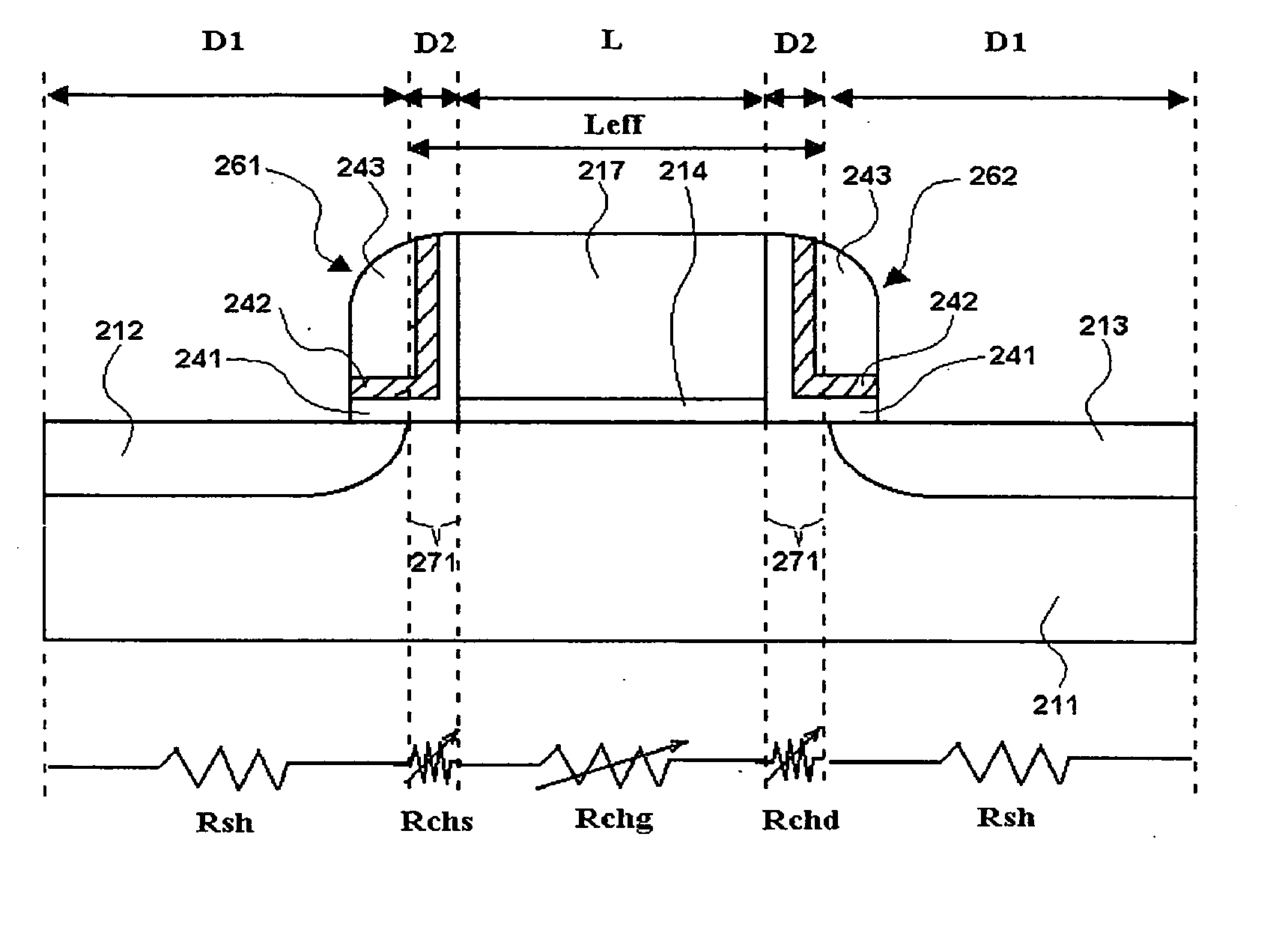
[0133] The present invention provides a characteristic evaluating method of obtaining a resistance value of the offset region (hereinafter, appropriately referred to as “offset resistance value”) by subtracting the resistance value of the channel region just below the gate electrode and the resistance value of the diffusion regions from the resistance value between two diffusion regions. The resistance value between the two diffusion regions, the resistance value of the channel region just below the gate electrode, and the resistance value of the diffusion re...

second embodiment

[0191] An embodiment of a model parameter extracting apparatus for a semiconductor memory element according to the present invention (hereinafter, appropriately referred to as “inventive apparatus”) will be described with reference to the drawings.

[0192] The inventive apparatus of the second embodiment has the function of executing the semiconductor memory element characteristic evaluating method and the model parameter extracting method according to the first embodiment.

[0193] As an example of the configuration of the inventive apparatus, an apparatus for evaluating characteristics of the semiconductor memory element and a model parameter extracting apparatus as shown in FIG. 22 can be mentioned. The configuration example is constructed by a PC or workstation 301 as a measurement controlling apparatus, a DC source / monitor 302a and an auto-prober 302b as a measuring apparatus, and a wafer 303 as an object to be measured.

[0194] The more-concrete configuration will be described wit...

second modification

(Second Modification)

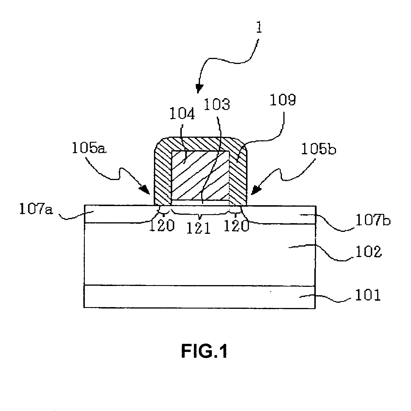
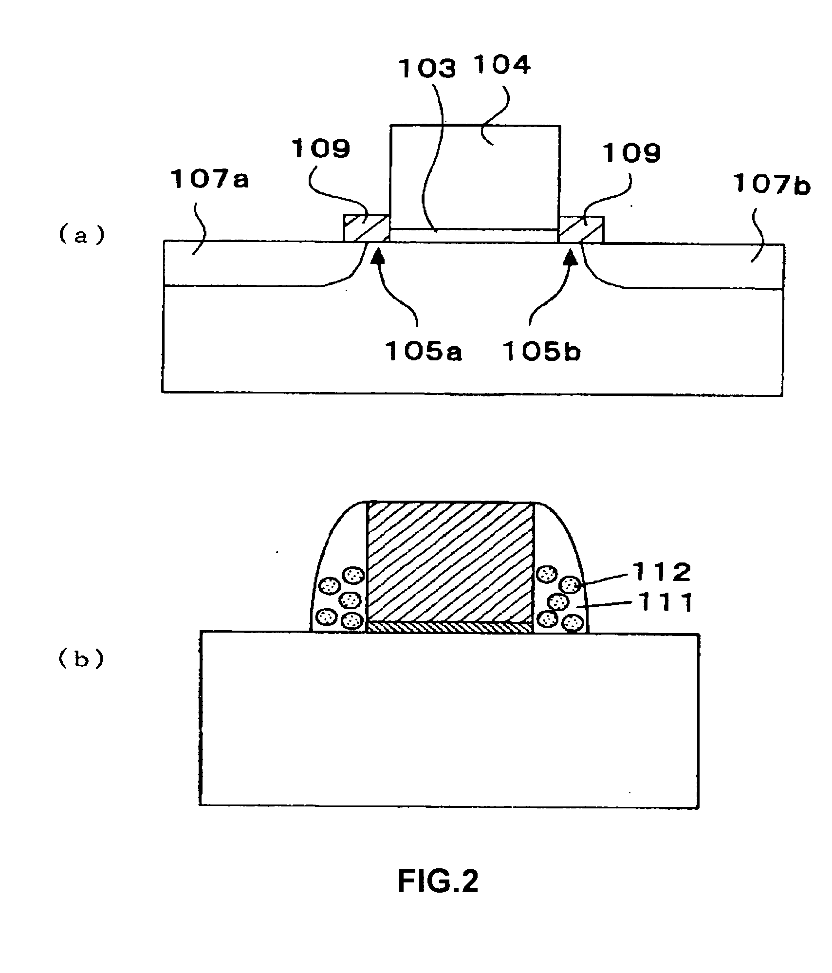
[0204] The memory functional element 262 in a semiconductor memory element of a second modification has a shape in which, as shown in FIG. 24, the silicon nitride film 242 as the charge retaining film has an almost constant thickness and is disposed almost parallel with the surface of the gate insulating film 214 (region 281) and, further, disposed almost parallel with a side surface of the gate electrode 217 (region 282).

[0205] In the case where a positive voltage is applied to the gate electrode 217, an electric line 283 of force in the memory functional element 262 passes through the silicon nitride film 242 twice (portions corresponding to the regions 282 and 281) as shown by the arrows. When a negative voltage is applied to the gate electrode 217, the direction of the electric line of force is reversed. The dielectric constant of the silicon nitride film 242 is about 6 and the dielectric constant of the silicon oxide films 241 and 243 is about 4. Therefore...


PUM


Abstract

A characteristic evaluating method of precisely obtaining a resistance value of an offset region in a semiconductor memory element constructed so that the resistance value of the offset region positioned below a memory function element formed on one side or both sides of a gate electrode changes according to an amount of charges or a polarization state of charges accumulated in said memory function element includes: a step of obtaining each of a resistance value between two diffusion regions inclusive formed on both sides of a channel region disposed just below the gate electrode of the semiconductor memory element via a gate insulating film, a resistance value of the channel region, and a resistance value of the diffusion regions; and a step of calculating the resistance value of the offset region which isolates the channel region and the diffusion region from each other on the basis of a result of subtracting the resistance value of the channel region and the resistance value of the diffusion regions from the resistance value between the two diffusion regions.

Description

CROSS REFERENCE TO RELATED APPLICATIONS [0001] This Nonprovisional application claims priority under 35 U.S.C. § 119(a) on Patent Application No. JP2003-400231 filed in Japan on 28 Nov. 2003, the entire contents of which are hereby incorporated by reference. BACKGROUND OF THE INVENTION [0002] 1. Field of the Invention [0003] The present invention relates to a method and apparatus for extracting a model parameter for a circuit simulation for a semiconductor memory element. More particularly, the present invention relates to a method of calculating a resistance value of an offset region in a semiconductor memory element having a gate electrode formed over a semiconductor layer via a gate insulating film, a channel region disposed just below the gate electrode via the gate insulating film, two diffusion regions formed on the both sides of the channel region, a memory function element formed on one side or both sides of the gate electrode and having a charge retaining function, and an o...

Claims


Application Information

Patent Timeline
IPC IPC(8): G11C11/34G11C16/04H01L29/00G11C16/26H01L21/8247H01L27/115H01L29/788H01L29/792
CPCG11C16/26G11C16/0425
Inventor HOSHINO, KOZOIWATA, HIROSHISHIBATA, AKIHIDE
Owner XENOGENIC DEV LLC
Why Eureka
Try Eureka