Dynamic threshold voltage MOSFET on SOI

a threshold voltage and dynamic technology, applied in the direction of transistors, electrical apparatus, semiconductor devices, etc., can solve the problems of increasing the integration density compromising the quality of portability, and putting severe constraints on the power consumption of the integrated circuit, etc., to achieve high performance

Active Publication Date: 2005-06-09
GLOBALFOUNDRIES US INC
View PDF6 Cites 51 Cited by
  • Summary
  • Abstract
  • Description
  • Claims
  • Application Information

AI Technical Summary

Benefits of technology

[0008] It is therefore an object of the present invention to provide a transistor structure capable of high performance at low power supply voltages.

Problems solved by technology

However, portable devices must have power supplies which do not significantly compromise the quality of portability, such as by the size and / or weight of batteries.
Therefore, a severe constraint is placed on power consumption of the integrated circuits and the transistors therein to provide adequate periods of service of the portable devices between battery replacement or recharging.
Even in non-portable devices, increased integration density is accompanied by increased power dissipation density.
Even though power dissipated by a single transistor may seem quite small, the power consumption or dissipation per unit of chip area increases with integration density.
In particular, while field effect transistors (e.g. MOSFETs) have become the technology of choice for all but the highest switching speeds, the transition time between “on” and “off” states, sometimes referred to as the slew rate, is severely degraded as power supply voltage is reduced; largely because of the capacitive load presented by field effect transistor gates.
While field effect transistors can be designed to operate satisfactorily at voltages which are somewhat reduced, they cannot be scaled to lower voltages as readily as power supplies.
In particular, the threshold voltage cannot be scaled by the same amount as power supply voltage because of sub-threshold leakage and the low limit for the sub-threshold output voltage swing.
Additionally, scaling of MOSFETs may cause them to be more delicate and susceptible to damage from breakdown due to static charge, coupled noise and the like.
Accordingly, it is an extreme challenge to scale the power supply voltage, improve the circuit speed and limit the leakage current simultaneously.
However, the principal disadvantage of this transistor design is that because gate bias is applied to the transistor body, the leakage current of the forward biased p-n junction at the source increases dramatically when the power supply voltage is greater than 0.7V; effectively limiting the power supply voltage to that value; a value which increases noise susceptibility and does not support sufficient voltage overdrive for optimal or potential switching speed.

Method used


Image

  • Dynamic threshold voltage MOSFET on SOI
  • Dynamic threshold voltage MOSFET on SOI
  • Dynamic threshold voltage MOSFET on SOI

Examples


Embodiment Construction

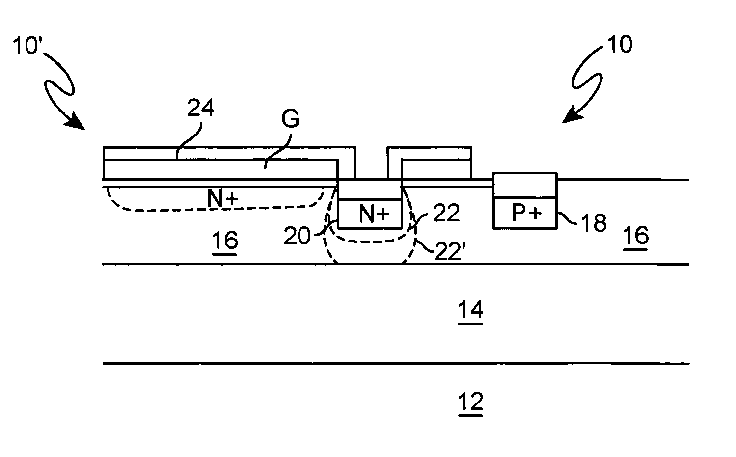
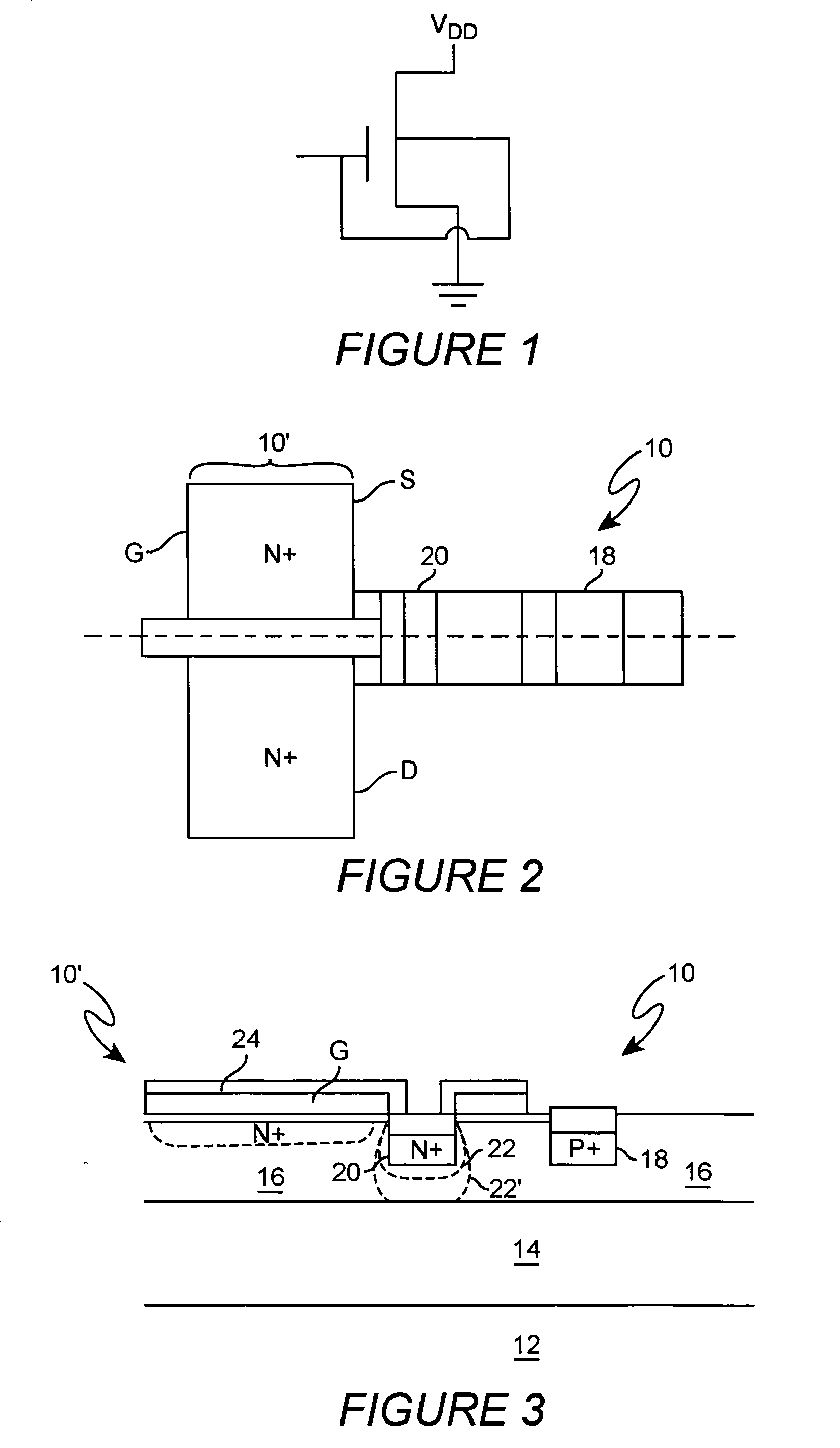
[0017] Referring now to the drawings, and more particularly to FIG. 2 and FIG. 3, plan and cross-sectional views of a DTMOSFET in accordance with the invention is shown. While a PMOS transistor is shown, it is to be understood that the principles of the invention are equally applicable to NMOS devices simply by reversing the conductivity types of the illustrated regions. It should also be appreciated that the principles of the invention and the implementation thereof is completely independent of the design of the remainder of the transistor and performance enhancing structures such as halo and extension implants can be designed and implemented freely, consistent with the practice of the invention. Therefore, such possible structures which are not important to the practice of the invention are to be considered as represented in the simplified form of the source S and drain D illustrated in the Figures.

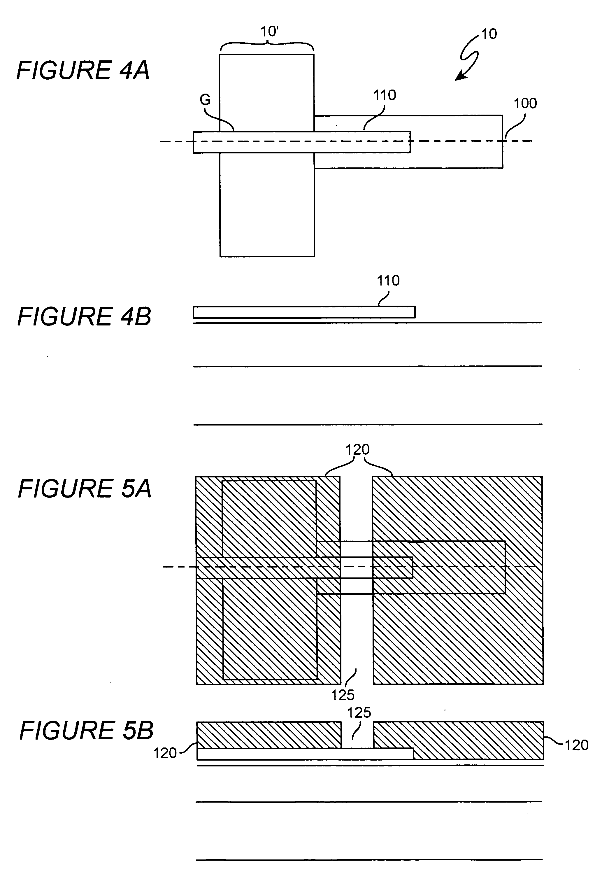
[0018] The transistor in accordance with the invention is preferably formed on a s...


PUM


Abstract

Provision of a body control contact adjacent a transistor and between the transistor and a contact to the substrate or well in which the transistor is formed allows connection and disconnection of the substrate of the transistor to and from a zero (ground) or substantially arbitrary low voltage in accordance with control signals applied to the gate of the transistor to cause the transistor to exhibit a variable threshold which maintains good performance at low supply voltages and reduces power consumption/dissipation which is particularly advantageous in portable electronic devices. Floating body effects (when the transistor substrate in disconnected from a voltage source in the “on” state) are avoided since the substrate is discharged when the transistor is switched to the “off” state. The transistor configuration can be employed with both n-type and p-type transistors which may be in complementary pairs.

Description

BACKGROUND OF THE INVENTION [0001] 1. Field of the Invention [0002] The present invention generally relates to the design and fabrication of transistors suitable for high density integration and, more particularly, to transistors capable of high performance even when operated at reduced voltages, such as in integrated circuits for portable devices. [0003] 2. Description of the Prior Art [0004] The possibility of increased chip functionality and performance and economy of manufacture of integrated circuits has provided substantial pressure toward higher integration density of integrated circuits. By the same token, greater chip functionality has also led to the development of many portable devices of small size such as so-called personal digital assistants, portable telephones with enhanced (e.g. video) functions and the like. However, portable devices must have power supplies which do not significantly compromise the quality of portability, such as by the size and / or weight of batte...

Claims


Application Information

Patent Timeline
Patent Type & Authority Applications(United States)
IPC IPC(8): H01L27/08H01L21/8238H01L27/085H01L27/092H01L27/12H01L29/745H01L29/78H01L29/786
CPCH01L29/783
Inventor CHEN, XIANGDONGCHIDAMBARRAO, DURESETIWANG, GENG
Owner GLOBALFOUNDRIES US INC
Why Eureka
Try Eureka