

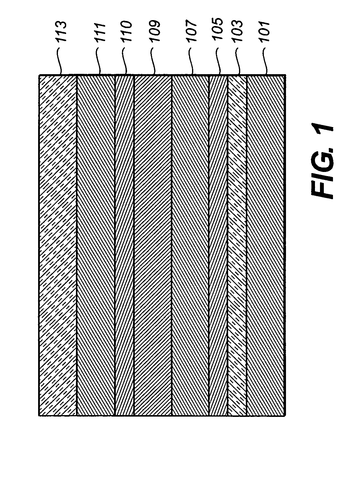
Organic element for electroluminescent devices
a technology of electroluminescent devices and organic elements, which is applied in the direction of discharge tube luminescnet screens, other domestic articles, natural mineral layered products, etc., can solve the problems of large loss of efficiency and performance limitations, and hinder many desirable applications
- Summary
- Abstract
- Description
- Claims
- Application Information
AI Technical Summary
Benefits of technology
Problems solved by technology
Method used
Image

Examples
synthetic example 1
Preparation of Inv-2
[0146]
[0147] 4,4′-Bis(phenylethynyl)biphenyl was prepared by the following procedure (R×n−1). A mixture of 12.0 g (0.030 mol) of 4,4′-diiodobiphenyl, 150 mL of piperidine, and 200 mL of acetonitrile was deaerated by sparging with argon, and 0.40 g (0.6 mmol) of bis(triphenylphosphine) palladium dichloride and 0.25 g (1.3 mmol) of copper (I) iodide were added. To the resulting stirred solution at room temperature was added 6.04 g (0.059 mol) of phenylacetylene via a syringe. The reaction mixture was held at room temperature for 30 min, and heated at 60° C. for 3 h. The precipitated product was collected by filtration of the cooled reaction mixture, and was washed successively with acetonitrile and dichloromethane until the solid was colorless. Yield: 8.5 g (81%). FD-MS m / z 354+ (M+).
[0148] Inv-2 (2′,2″″,3′,3″″,5′,5″″,6′,6″″-octaphenyl-p-sexiphenyl) was prepared from 4,4′-bis(phenylethynyl)biphenyl (R×n−2) by the following method. A mixture of 5.00 g (0.014 mol)...
example 1
DEVICE EXAMPLE 1
[0150] An EL device (Sample 1) satisfying the requirements of the invention was constructed in the following manner: [0151] 1. A glass substrate coated with an 85 nm layer of indium-tin oxide (ITO) as the anode was sequentially ultrasonicated in a commercial detergent, rinsed in deionized water, degreased in toluene vapor and exposed to oxygen plasma for about 1 min. [0152] 2. Over the ITO was deposited a 1 nm fluorocarbon (CFx) hole-injecting layer (HIL) by plasma-assisted deposition of CHF3. [0153] 3. A hole-transporting layer (HTL) of N,N′-di-1-naphthyl-N,N′-diphenyl-4,4′-diaminobiphenyl (NPB) having a thickness of 75 nm was then evaporated from a tantalum boat. [0154] 4. A 35 nm light-emitting layer (LEL) of Inv-1 and a green phosphorescent dopant, (Ir(ppy)3, fac-tris(2-phenylpyridinato-N,C2′)iridium(III), 6 wt %) were then deposited onto the hole-transporting layer. These materials were also evaporated from tantalum boats. [0155] 5. A hole-blocking layer of bis(...
example 2
DEVICE EXAMPLE 2
[0162] An EL device, Sample 7, satisfying the requirements of the invention was constructed in the same manner as Sample 1 described above, except Inv-2 was used in place of Inv-1. Samples 8, 9, and 10 were prepared in the same manner as Sample 7, except emitter Ir(Ppy)3 was used at level indicated in Table 2. Sample 11 was constructed in the same manner as Sample 7, except host Com-1 (4,4′-bis(carbazol-9-yl)biphenyl, CBP) was used in place of Inv-2.
[0163] The cells thus formed were tested for luminance, efficiency and color CIE coordinates at an operating current of 20 mA / cm2 and the results are reported in Table 2.
TABLE 2Evaluation Results for EL devices.GreenDopantLumianceEfficiencySampleHostLevel (%)(cd / m2)(W / A)CIExCIEyType7Inv-2432830.1040.3180.621Invention8Inv-2641130.1310.3160.624Invention9Inv-2842370.1340.3180.623Invention10Inv-20580.0030.1990.315Comparison11Com-1639050.1250.3130.621Comparison
[0164] As can be seen from Table 2, all tested EL devices incorp...
PUM
| Property | Measurement | Unit |
|---|---|---|
| thick | aaaaa | aaaaa |
| thickness | aaaaa | aaaaa |
| work function | aaaaa | aaaaa |
Abstract
Description
Claims
Application Information