Semiconductor device and method of manufacturing the same

a semiconductor and resistor technology, applied in the field of semiconductor devices, can solve the problems of reducing the resolution affecting the quality of the second resist pattern, and increasing the density of the wiring pattern,

Inactive Publication Date: 2005-06-09
RENESAS ELECTRONICS CORP
View PDF3 Cites 28 Cited by
  • Summary
  • Abstract
  • Description
  • Claims
  • Application Information

AI Technical Summary

Benefits of technology

[0032] As described above, according to the present invention, the annealing treatment, the plasma treatment, the UV treatment, the organic solvent treatment or the like may be conducted as the pre-treatment for forming the resist pattern, whereby the reaction inhibiting materials such as amine, etc. remaining in wafer, particularly in the low dielectric-constant interlayer insulating film can be surely removed. Furthermore, a modified film having modified composition, density or bond state is formed by conducting the annealing treatment or the UV treatment on a face layer of the insulating film, the barrier film or the etching stop film confronting the via hole or the wiring trench patter...

Problems solved by technology

With the damascene process described above, the density of the wiring pattern can be increased, however, a wiring delay problem would occur due to the parasitic capacity between wiring patterns if the wiring patterns are close to each other.
Therefore, there is a problem that the resolution of the second resist pattern 1b is lowered by the reaction inhibiting materials.
However, the reaction inhibiting materials infiltrating into the interlayer insulating film exudes into the resist to deactivate the acid catalyst and thus suppress the chemical reactions in the resist, so that the resist at a part of the wire trench patterns 10, particularly the resist in the neighborhood of the via holes 9 is not sufficiently removed and thus remains there.
Therefore, there occurs a problem that reliability of the completed wires is reduced.
This problem also occurs when SiO2 is used for the interlaye...

Method used


Image

  • Semiconductor device and method of manufacturing the same
  • Semiconductor device and method of manufacturing the same
  • Semiconductor device and method of manufacturing the same

Examples


example 1

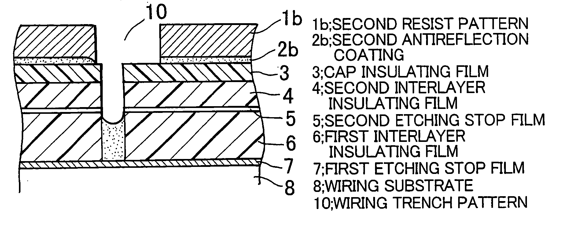
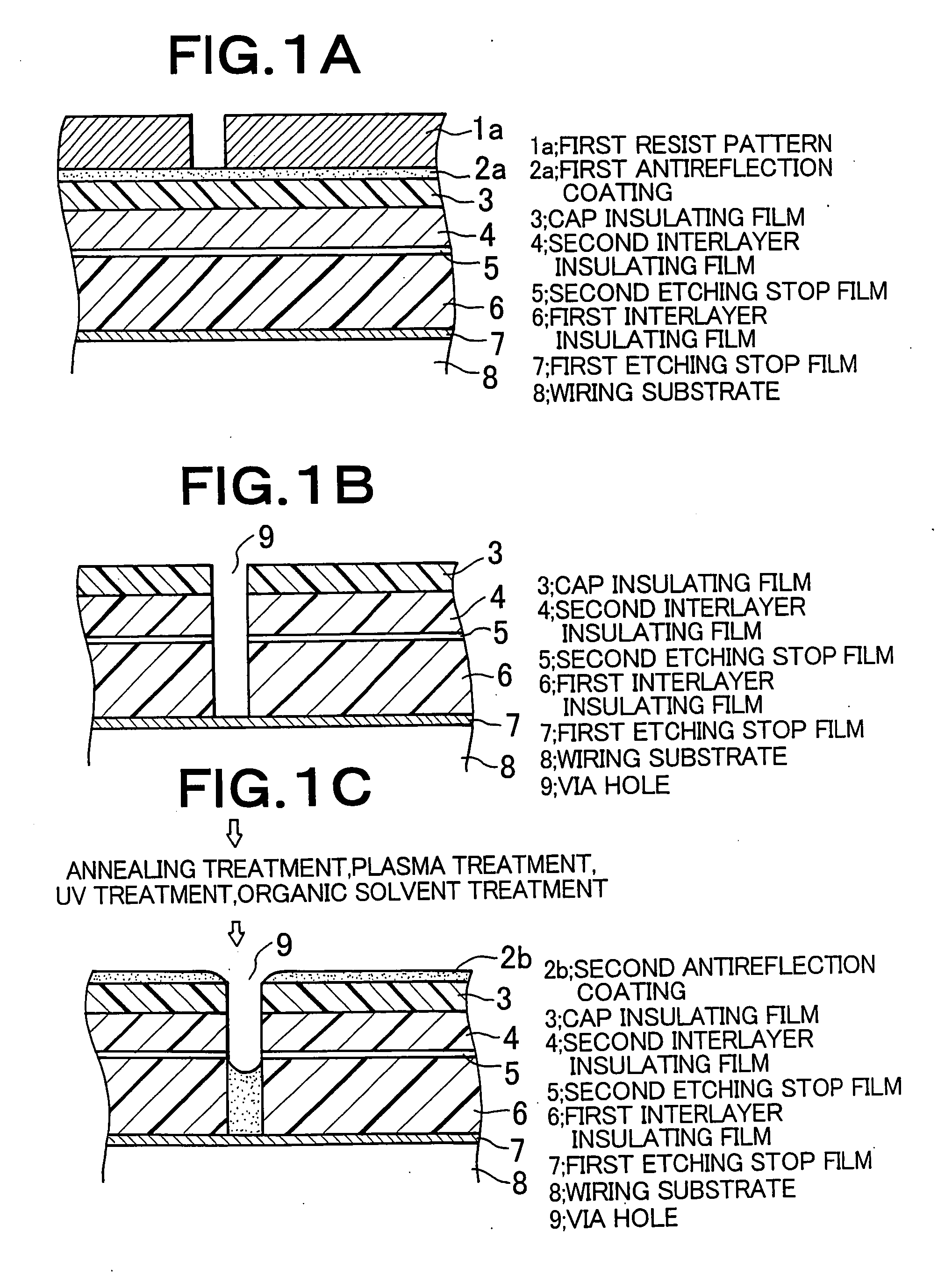
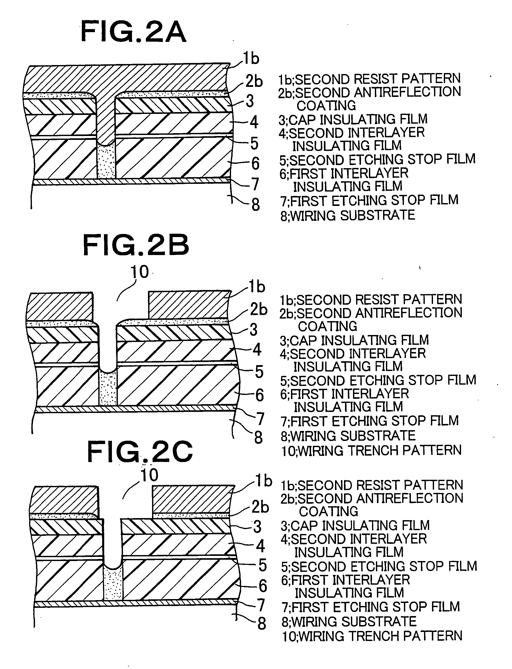
[0077] A first example of a semiconductor device and its manufacturing method to which the present invention relates will be described with reference to FIGS. 1A to 10C.

[0078]FIGS. 1A to 3C are cross-sectional views showing the procedure of a via-first process of the first example, and as a matter of convenience of drawing, it is illustrated as being divided into plural diagrams. FIG. 4 is a diagram showing the construction of a gas analysis system to set the condition of an annealing treatment. FIGS. 5A and 5B show analysis results thereof. FIGS. 6A to 7B are diagrams showing the difference between a case where SiO2 is used as an interlayer insulting film and another case where a low dielectric-constant film is used as an interlayer insulting film and FIG. 8 is a diagram showing the difference in effect of amine component due to the difference in via pattern interval. Further, FIGS. 9A and 9B are diagrams showing the effect of a UV treatment, and FIGS. 10A to 10C show the effect o...

example 2

[0106] A second example of the semiconductor device and its manufacturing method to which the present invention relates will be described with reference to FIGS. 11A to 13C.

[0107]FIGS. 11A to 13C are cross-sectional views showing the procedure of a via-first process according to the second example, and as a matter of convenience of drawing, it is illustrated as being divided into plural diagrams. This example is characterized in that the antireflection coating is perfectly filled in the via holes, and the structure and the manufacturing method of the other portions are the same as the first example.

[0108] First, as in the case of the first example, as shown in FIG. 11A, the lower-layer wire of Cu or the like is formed on the wiring substrate 8 by a well known method, and then the first etching stop film 7, the first interlayer insulating film 6, the second etching stop film 5, the second interlayer insulating film 4 and the cap insulating film 3 are successively formed by the CVD ...

example 3

[0116] Next, the semiconductor device and its manufacturing method according to a third example of the present invention will be described with reference to FIGS. 14A to 16. FIGS. 14A to 16 are cross-sectional views showing the procedure of a dual hard mask process according to the third example, and as a matter of convenience of drawing, it is illustrated as being divided into plural diagrams. This example is characterized in that the wiring trench pattern is formed by using a hard mask.

[0117] As in the case of the first and second examples, as shown in FIG. 14A, the lower-layer wire of Cu or the like is formed on the wiring substrate 8 by a well-known method, and then the first etching stop film 7, the first interlayer insulating film 6, the second etching stop film 5 and the second interlayer insulating film 4 are successively formed by using the CVD method, the plasma CVD method or the like. Subsequently, in this embodiment, a hard-mask film lower portion 13 and a hard mask fil...


PUM


Abstract

A method of manufacturing a semiconductor device having a damascene structure contains a process of forming a first interlayer insulating film (6) and a second interlayer insulating film (4) formed of a low dielectric-constant film on a substrate, forming via holes (9) by using a first resist pattern (1a) formed on the second interlayer insulating film, conducting an organic peeling treatment using organic peeling liquid containing amine components and then forming a second resist pattern (1b) on the second interlayer insulating film. After the wet treatment, before a second antireflection coating (2b) is coated so as to be located below the second resist pattern is coated, at least one of an annealing treatment, a plasma treatment, a UV treatment and an organic solvent treatment is carried out to remove amine components which inhibit the catalysis reaction of acid occurring in the resist at the light exposure, thereby preventing degradation of the resolution of the second resist pattern (1b).

Description

BACKGROUND OF THE INVENTION [0001] 1. Field of the Invention [0002] The present invention relates to a semiconductor device and a method of manufacturing the same, and particularly to a semiconductor device having a damascene structure and a method of manufacturing the same. [0003] 2. Description of the Related Art [0004] In connection with enhancement in the integration of semiconductor devices and reduction in chip size, miniaturization of wires and multi-layered wiring have been recently promoted. As a method of forming a multi-layered wiring structure is generally carried out a so-called damascene process in which Cu is embedded into via holes and wiring trench patterns at the same time and then surface flattening is carried out by using CMP (Chemical Mechanical Polishing) method to form wires. With the damascene process described above, the density of the wiring pattern can be increased, however, a wiring delay problem would occur due to the parasitic capacity between wiring pa...

Claims


Application Information

Patent Timeline
IPC IPC(8): H01L21/027H01L21/311H01L21/768G03F7/38
CPCH01L21/02063H01L21/31116H01L21/31138H01L21/76807H01L21/76831H01L21/76811H01L21/76825H01L21/76828H01L21/76808
Inventor NAGAHARA, SEIJISHIBA, KAZUTOSHIHAMANAKA, NOBUAKIUSAMI, TATSUYAYOKOYAMA, TAKASHI
Owner RENESAS ELECTRONICS CORP
Why Eureka
Try Eureka