SRAM device and a method of operating the same to reduce leakage current during a sleep mode

a technology of static random access memory and leakage current, which is applied in the field of memory devices, can solve the problems of unacceptable current leakage, low leakage rate, and low leakage rate, and achieve the effects of reducing subthreshold current leakage, reducing total leakage current, and increasing diode gate leakag

Active Publication Date: 2005-06-16
TEXAS INSTR INC
View PDF1 Cites 59 Cited by
  • Summary
  • Abstract
  • Description
  • Claims
  • Application Information

AI Technical Summary

Benefits of technology

[0013] The present invention allows optimization of the trade-off between reducing subthreshold current leakage and increasing diode gate leakage when a threshold voltage is increased with back bias for both n-channel and p-channel transistors. The present invention may substantially minimize total leakage current including gate, diode, and subthreshold currents by both raising a low operating voltage of the SRAM array relative to Vp-well and lowering a high operating voltage of the SRAM array relative to Vn-well. As transistor miniaturization continues, the present invention may reduce concerns over diode and gate leakage by allowing heavier doping for a higher threshold voltage or improved control of short channel effects. Thus, the present advantageously allows the use of shorter gate lengths while maintaining about the same Ioff. The present invention may allow optimization of the array high supply voltage VADD, the array low supply voltage VASS and a well voltage as set values for a general technology class of transistors. Additionally, the present invention may allow further optimization of the SRAM array voltages through adjustments and refinements based on specific transistor characteristics.
[0014] In another aspect, the present invention provides a method of operating an SRAM device including (1) employing in an integrated circuit an SRAM array coupled to row peripheral circuitry by a word line and coupled to column peripheral circuitry by bit lines and (2) providing both an array high supply voltage VADD that is lower than a high operating voltage VDD and an array low supply voltage VASS that is higher than a low operating voltage VSS to the SRAM array during a sleep mode. Through this method of operating, current leakage during the sleep mode may be reduced.

Problems solved by technology

ROM, however, does not accommodate writing.
SRAM devices, however, are often employed within battery-powered wireless apparatus where power consumption is an important design parameter.
As transistor size continues to diminish (e.g., 90 nm transistors), current leakage may be unacceptably high even during standby mode, requiring a transition to a still lower power consumption level, sleep mode, or data retention mode, to conserve power adequately.
Even in sleep mode, however, current leakage is a concern.
Typically, as voltage between the source or drain and the back gate increases, the diode leakage current also increases.
As mentioned, the increased back bias incurs an increase in the diode leakage current that reduces or negates the benefit of reduced subthreshold current.
Thus, a tradeoff often occurs between increasing the voltage of the well that increases the threshold voltage and reduces the subthreshold leakage current, the Ioff current, that at the same time increases the diode leakage current.
This heavier doping limits the subthreshold current increase with scaling but increases the diode leakage.

Method used


Image

  • SRAM device and a method of operating the same to reduce leakage current during a sleep mode
  • SRAM device and a method of operating the same to reduce leakage current during a sleep mode
  • SRAM device and a method of operating the same to reduce leakage current during a sleep mode

Examples


Embodiment Construction

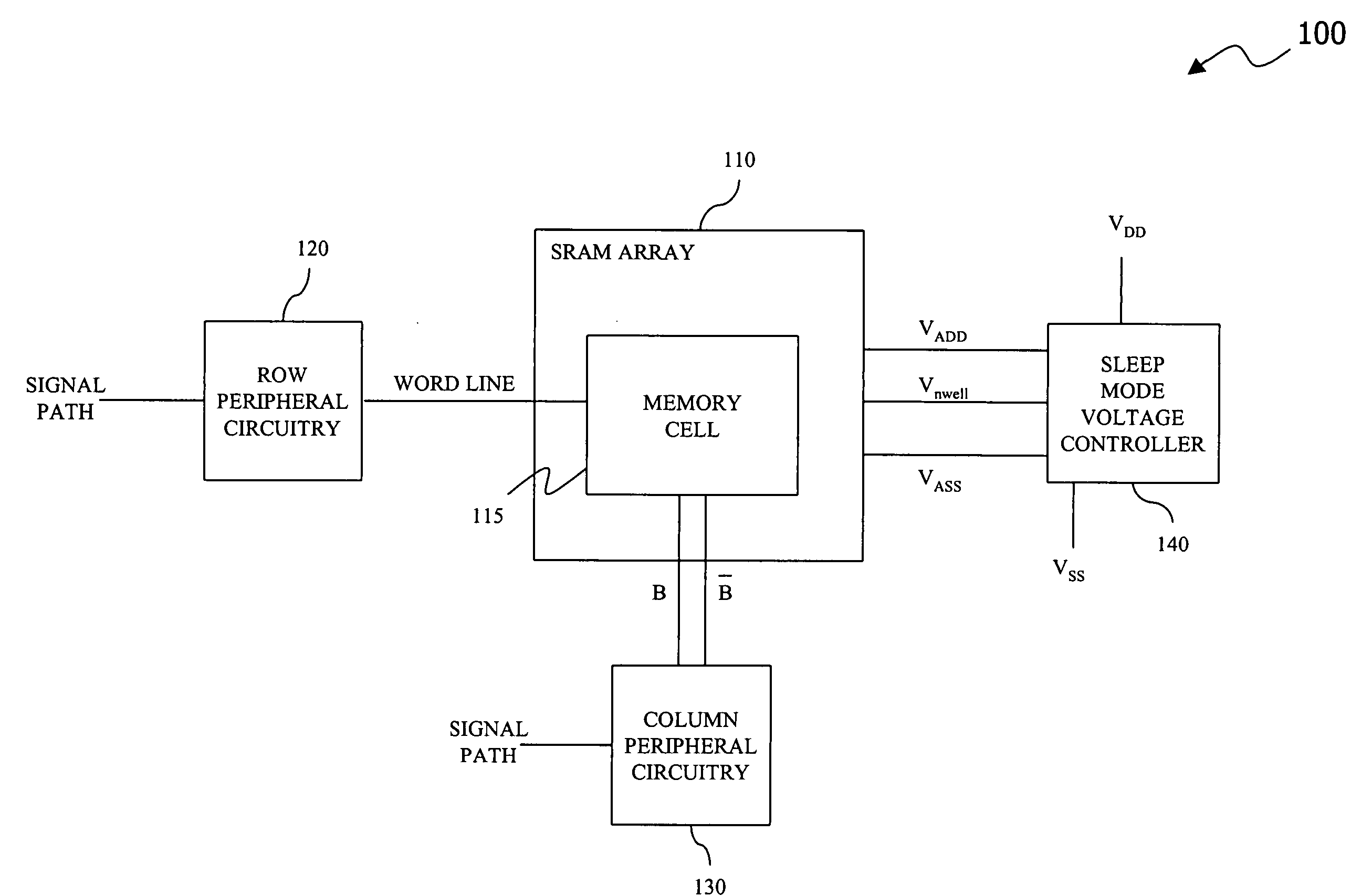
[0020] Referring initially to FIG. 1, illustrated is a circuit diagram of an embodiment of an SRAM device, generally designated 100, constructed according to the principles of the present invention. The SRAM device 100 includes an SRAM array 110, row peripheral circuitry 120, column peripheral circuitry 130 and a sleep mode voltage controller 140. Typically, the SRAM array 110 includes multiple memory cells organized in a matrix of columns and rows with corresponding multiple word lines and bit lines. For example, the SRAM array 110 may have 256 columns and 256 rows of memory cells. For ease of discussion, however, only a single memory cell 115 of the SRAM array 110 is illustrated. Accordingly, a single word line and bit line pair are illustrated and discussed along with the associated row and column peripheral circuitry 120, 130.

[0021] The SRAM device 100 may be a memory component for an associated microprocessor, digital signal processor (DSP), application-specific integrated cir...


PUM


Abstract

An SRAM device and a method of operating an SRAM device. In one embodiment, the SRAM device includes (1) an SRAM array coupled to row peripheral circuitry by a word line and coupled to column peripheral circuitry by bit lines and (2) a sleep mode voltage controller configured to provide both an array high supply voltage VADD that is lower than a high operating voltage VDD and an array low supply voltage VASS that is higher than a low operating voltage VSS to the SRAM array during a sleep mode.

Description

TECHNICAL FIELD OF THE INVENTION [0001] The present invention is directed, in general, to memory devices and, more specifically, to a Static Random-Access Memory (SRAM) device and a method of operation that reduces leakage current during a sleep mode. BACKGROUND OF THE INVENTION [0002] Different types of memory are used in electronic apparatus for various purposes. Read only memory (ROM) and random-access memory (RAM) are two such types of memory commonly used within computers for different memory functions. ROM retains its stored data when power is switched off and therefore is often employed to store programs that are needed for powering-up an apparatus. ROM, however, does not accommodate writing. RAM, on the other hand, allows data to be written to or read from selected addresses associated with memory cells and, therefore, is typically used during normal operation of the apparatus. [0003] Two common types of RAM are dynamic RAM (DRAM) and static RAM (SRAM). DRAM is typically use...

Claims


Application Information

Patent Timeline
Patent Type & Authority Applications(United States)
IPC IPC(8): G11C5/14G11C11/00G11C11/417G11C29/02
CPCG11C5/147G11C11/41G11C11/417G11C2029/5006G11C29/028G11C2029/0409G11C29/02
Inventor HOUSTON, THEODORE W.
Owner TEXAS INSTR INC
Why Eureka
Try Eureka