Method for the manufacture of micro structures

a micro-structure and manufacturing method technology, applied in the field of photolithographic processes, can solve the problems of difficult to meet the needs of sensitive components, difficult to meet the needs of vacuum systems and beam guidance systems, and limited photolithographic techniques of the day, and achieve the effect of reducing the width of the trench structur

Inactive Publication Date: 2005-06-16
IBM CORP
View PDF5 Cites 21 Cited by
  • Summary
  • Abstract
  • Description
  • Claims
  • Application Information

AI Technical Summary

Benefits of technology

[0013] It is therefore an object of the present invention to provide a m

Problems solved by technology

Today's photolithographical techniques are still restricted by the wavelength of the used exposure light to arrive at critical dimensions as small as possible.
However, this requires expensive vacuum systems and beam guidance systems.
In addition, problems can occur with sensitive components due to radiation damage in the substrate, because the high-energy particles can penetrate through the resist layers required for etching processes.
Usually, t

Method used


Image

  • Method for the manufacture of micro structures
  • Method for the manufacture of micro structures
  • Method for the manufacture of micro structures

Examples


Embodiment Construction

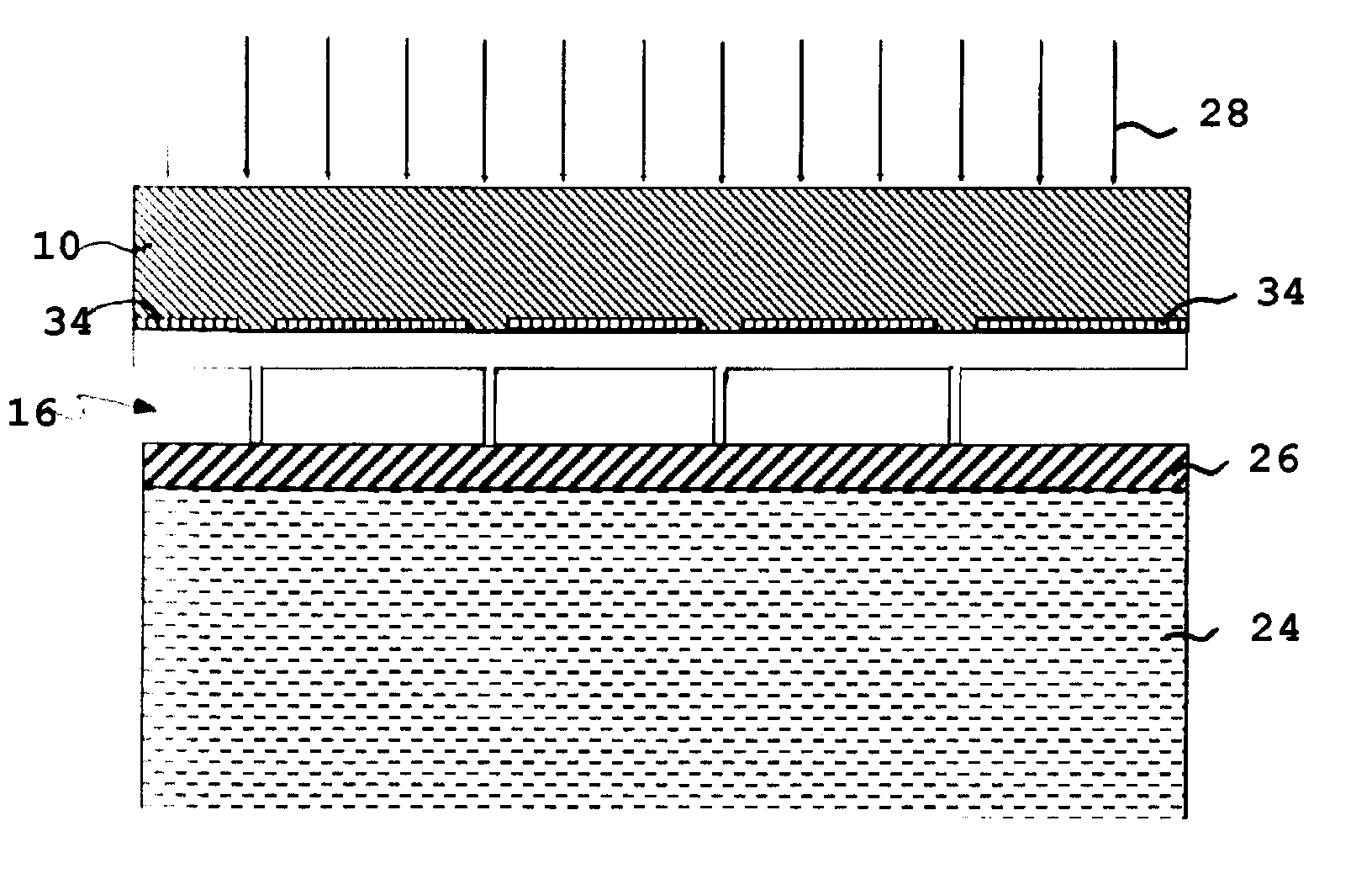
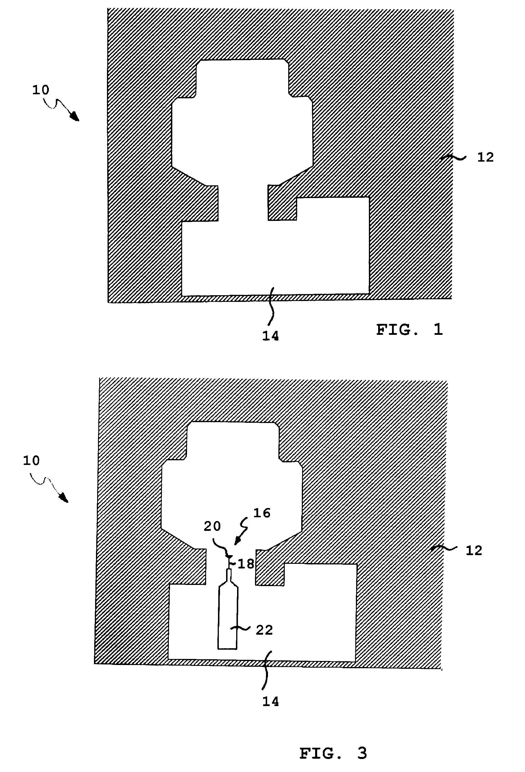
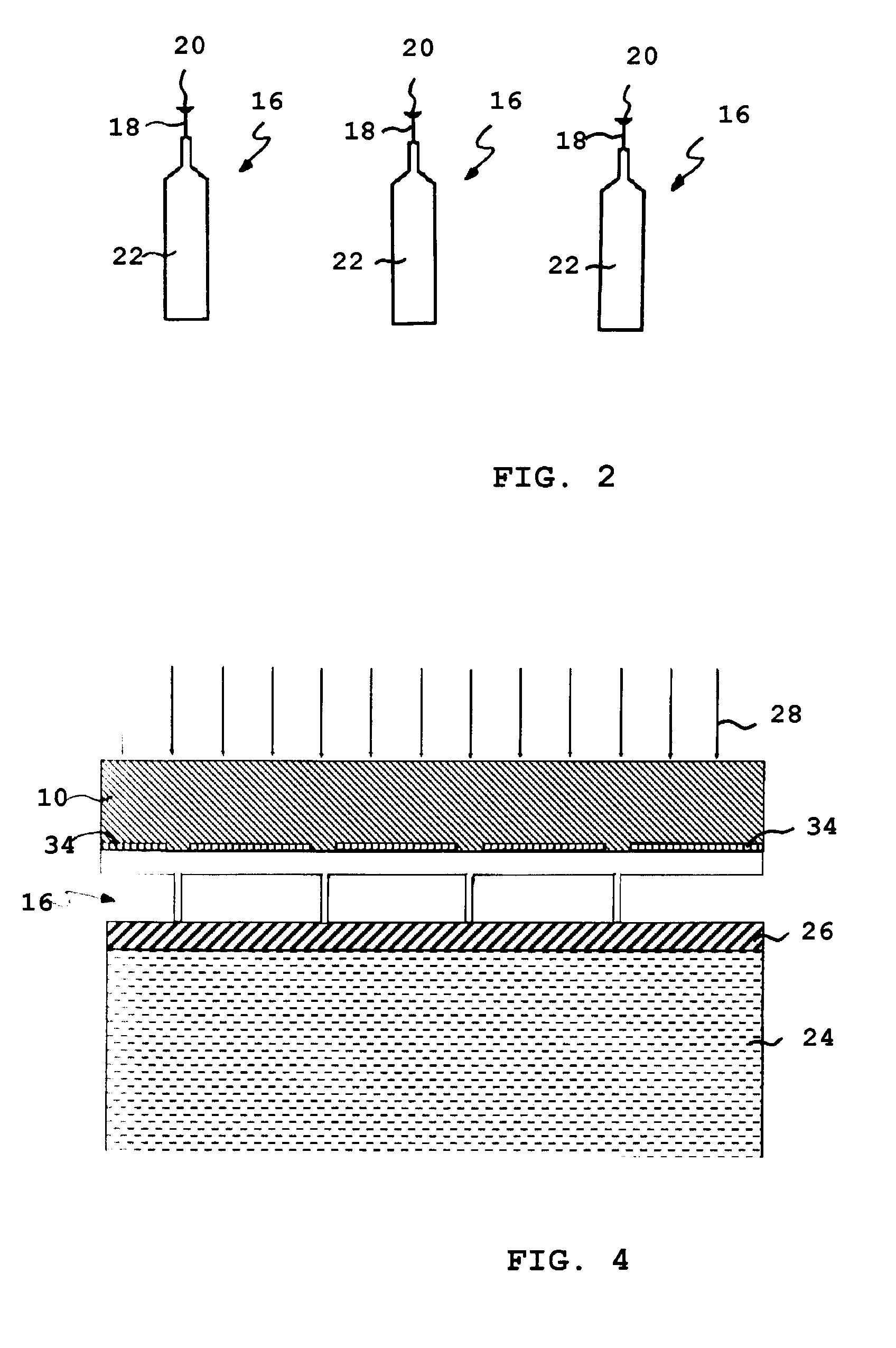
[0025] The proposed technology is a combination of mask photolithography and micro contact printing in order to produce metallic structures on a substrate, these structures having narrow dimensions and a very high aspect ratio, like, e.g., write pole and sensor on magnetic recording heads (thin film technology), MD trenches for capacitors and any other kind of narrow trenches used in Thin Film Technology (TFT), MD or micromechanics.

[0026] In the following, the invention will be described in more detail with respect to the formation of a P2 structure on wafers for standard magnetic recording heads. However, it has to be mentioned that the invention is not restricted to such a special process, but can be used to manufacture narrow dimensions on every substrate.

[0027] In manufacturing the P2 structure, the method according to the invention is used to stamp the necessary critical dimension geometry into the resist layer on top of the planarized layer, in the present case the write gap...


PUM

PropertyMeasurementUnit
Microstructureaaaaaaaaaa
Areaaaaaaaaaaa
Aspect ratioaaaaaaaaaa

Abstract

Method for the Manufacture of Micro Structures A method for the manufacture of micro structures in substrates is provided. The method uses a combination of photolithographic mask technology and micro contact printing.

Description

BACKGROUND OF INVENTION [0001] The present invention relates in general to photolitho-graphic processes. Specifically, the present invention is concerned with a process for the manufacture of metallic structures in a substrate having narrow dimensions. [0002] In semiconductor technology and in microelectronics, the dimensions of structures are becoming smaller and smaller. In memory production today, e.g., structures with a width of less than 200 nm are produced using optical lithography in combination with the masking technique. Photholithographic processes are vital steps in the fabrication of, e.g., semiconductor devices. In a photolitho-graphic process, an exposure light, usually ultraviolet (UV) light is used to expose a photoresist-coated semiconductor wafer through a mask (in the following called photomask). The purpose of the photolithographic process is to transfer a set of patterns representative of the circuit layer onto the wafer. The patterns on the photomask define the...

Claims


Application Information

Patent Timeline
IPC IPC(8): G03F7/20B81C1/00C23C30/00G03F1/08G03F7/00G11B5/31H01L21/027
CPCB82Y10/00G03F7/0002B82Y40/00
Inventor KRAUSE, RAINER KLAUSSCHMIDT, MARKUS
Owner IBM CORP
Why Eureka
Try Eureka