Optical apparatus and image production apparatus

a technology of optical apparatus and image, applied in the direction of instruments, optical elements, discharge tubes/lamp details, etc., can solve the problems of color blurring, difficulty in forming a clean image, and so on, and achieve the effect of reducing the difficulty of cleaning

Inactive Publication Date: 2005-06-23
SONY CORP
View PDF21 Cites 43 Cited by
  • Summary
  • Abstract
  • Description
  • Claims
  • Application Information

AI Technical Summary

Benefits of technology

[0016] It is an object of the present invention to provide an optical apparatus having a configuration and structure by which, even if heat is generated with optical elements in a diffraction grating-optical modulation apparatus or the like, lights emitted from the optical elements are less likely to suffer from displacement therebetween.

Problems solved by technology

As a result, color blurring or the like occurs, and it is difficult to form a clean image.
As reduction in size and enhancement of the resolution of a diffraction grating-optical modulation apparatus proceeds, the problem of such color blurring and so forth becomes further conspicuous.

Method used


Image

  • Optical apparatus and image production apparatus
  • Optical apparatus and image production apparatus
  • Optical apparatus and image production apparatus

Examples


embodiment 1

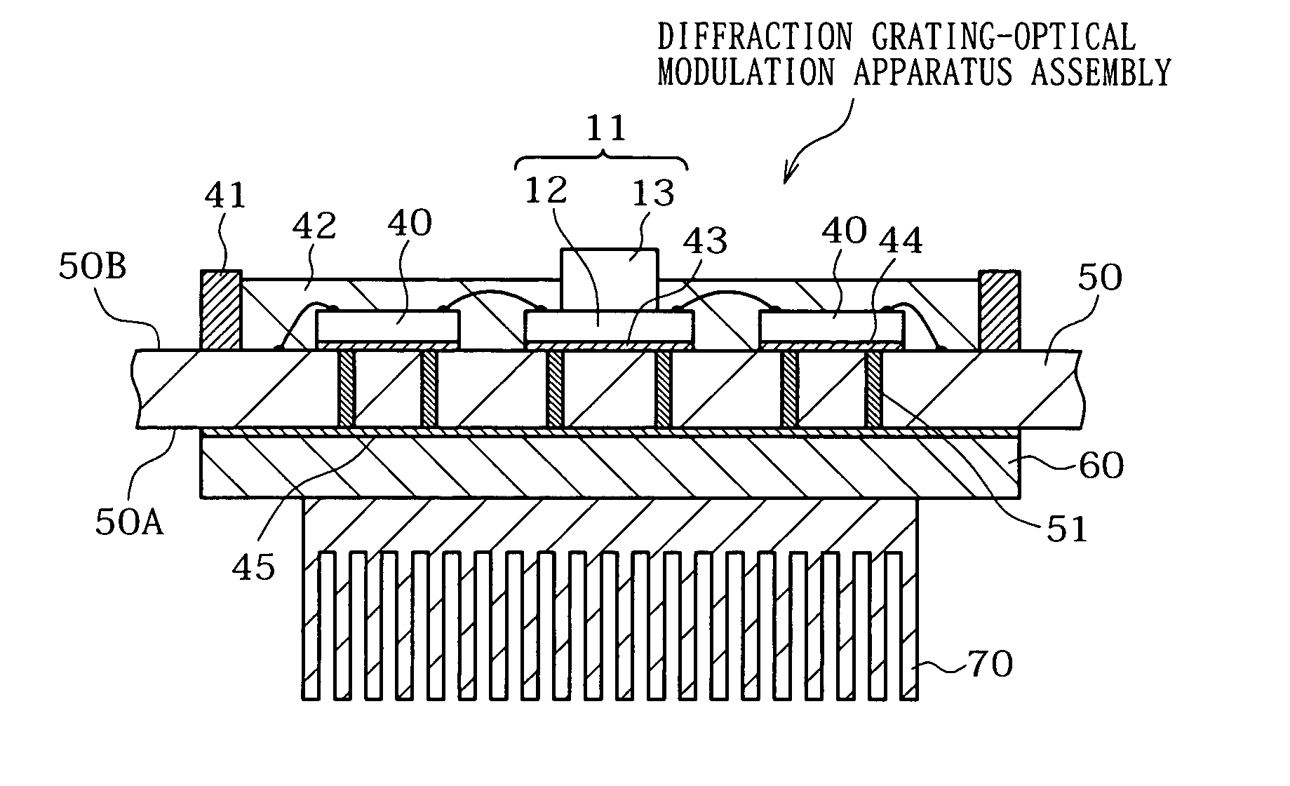
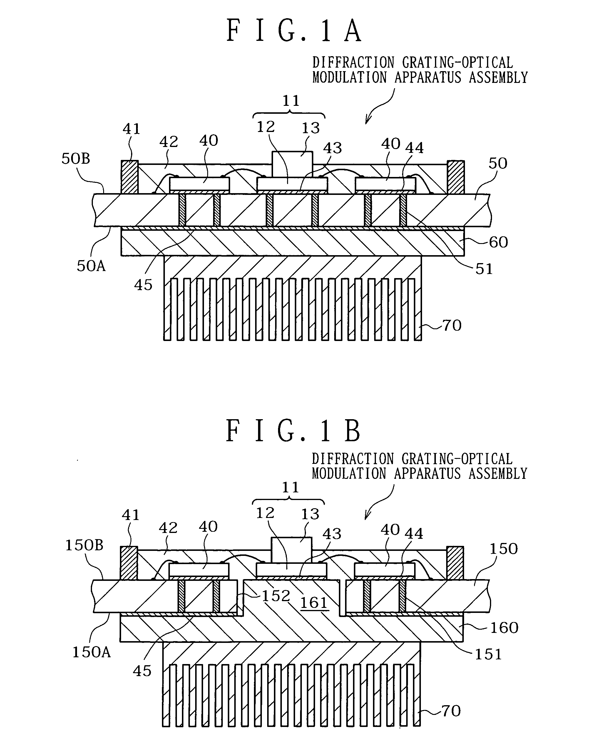
[0130] An embodiment 1 relates to an optical apparatus and an image production apparatus according to a first mode for carrying out the present invention. The optical apparatus of the embodiment 1 includes an optical element wherein a plurality of diffraction grating-optical modulation elements (GLV) are arrayed in a one-dimensional array. It is to be noted that, in the following description, the optical element is sometimes referred to as diffraction grating-optical modulation apparatus and the optical apparatus is sometimes referred to as diffraction grating-optical modulation apparatus assembly. Further, the image forming apparatus of the embodiment 1 includes the optical apparatus (diffraction grating-optical modulation apparatus assembly) and a light source (semiconductor laser) similarly to that shown in FIG. 12. A schematic partial sectional view of the optical apparatus (diffraction grating-optical modulation apparatus assembly) of the embodiment 1 is shown in FIG. 1A, and a...

embodiment 2

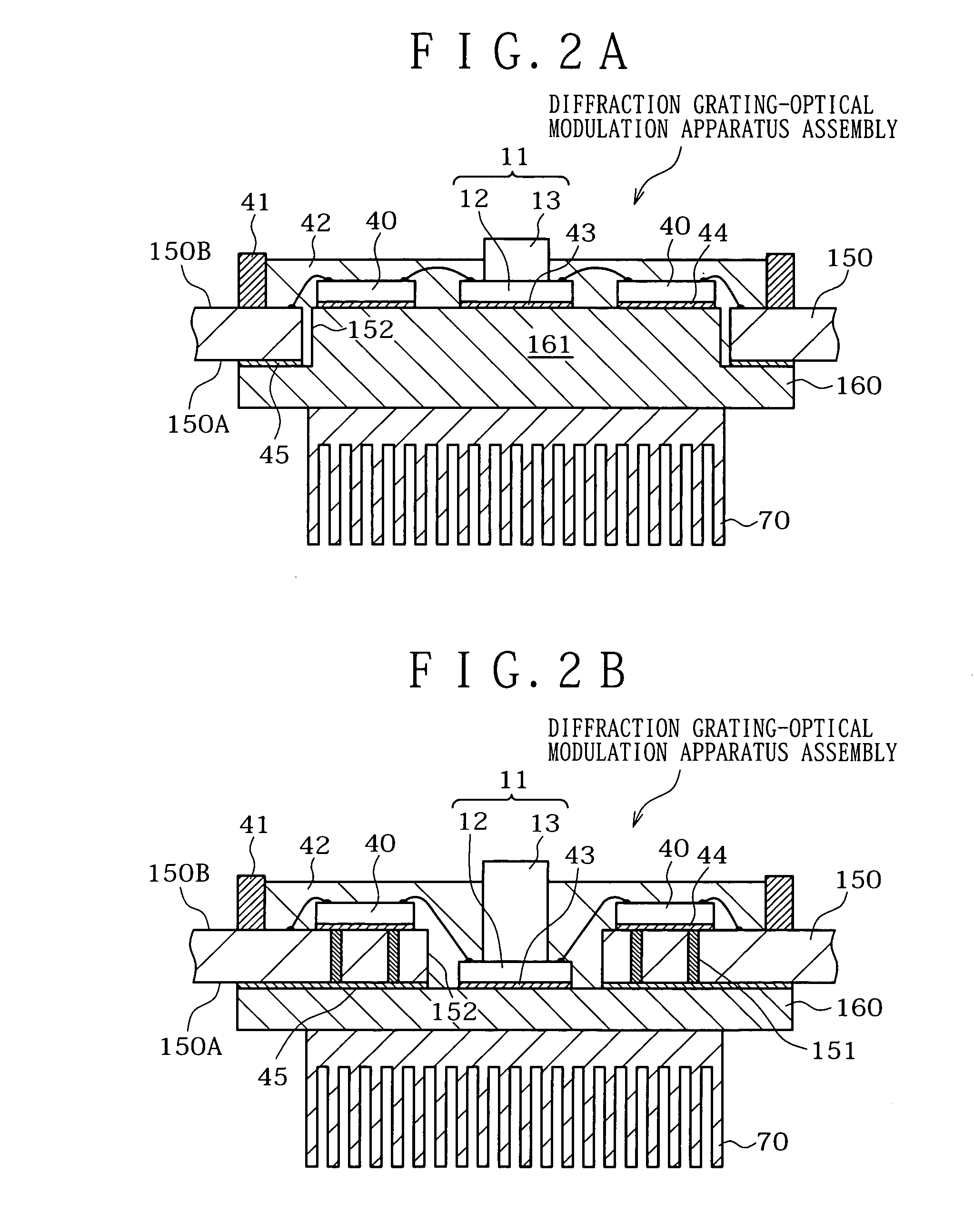
[0146] An embodiment 2 relates to an optical apparatus and an image forming apparatus according to a second mode for carrying out the present invention. Also the optical apparatus of the embodiment 2 particularly includes an optical element (diffraction grating-optical modulation apparatus) wherein a plurality of diffraction grating-optical modulation elements (GLV) are arrayed in a one-dimensional array. Also the image production apparatus of the embodiment 2 includes the optical apparatus (diffraction grating-optical modulation apparatus assembly) and a light source (semiconductor laser) similarly to that described hereinabove with reference to FIG. 12. A schematic partial sectional view of the optical apparatus (diffraction grating-optical modulation apparatus assembly) of the embodiment 2 is shown in FIG. 1B, and a schematic partial perspective view of a mounting substrate of the optical apparatus (diffraction grating-optical modulation apparatus assembly) is shown in FIG. 5A. F...

embodiment 3

[0158] An embodiment 3 is a modification to the embodiment 2. In the embodiment 2, the semiconductor chips 40 are attached to the face 150B of the mounting substrate 150. On the other hand, in the embodiment 3, the semiconductor chips 40 are attached to the portion (support member projection 161) of the support member 160 exposed in the opening 152 formed in the mounting substrate 150 by means of bonding agent 44 for die bonding as seen in FIG. 2A which shows a schematic partial sectional view of the optical apparatus (diffraction grating-optical modulation apparatus assembly). It is to be noted that a schematic partial perspective view of the mounting substrate 150 is same as that shown in FIG. 5A, and a schematic partial perspective view of the mounting substrate 150 and the support member 160 is similar to that shown in FIG. 5B. A schematic partial plan view of the mounting substrate 150 is shown in FIG. 7A.

[0159] Except such an attached state of the semiconductor chips 40 as ju...


PUM


Abstract

An optical apparatus is disclosed by which, even if heat is generated with optical elements in a diffraction grating-optical modulation apparatus, lights emitted from the optical elements is less likely to suffer from displacement therebetween. The optical apparatus includes an optical element, a mounting substrate, a support member, and a cooling/heat radiating member. The support member is attached to a first face of the mounting substrate while the optical element is attached to a second face of the mounting substrate. The cooling/heat radiating member is attached to the support member. The optical element and the support member are thermally connected to each other by a heat transmission element provided in the inside of the mounting substrate. The support member is made of a material having a thermal conductivity of 230 W/m·K or more.

Description

BACKGROUND OF THE INVENTION [0001] The present invention relates to an optical apparatus and an image production apparatus. [0002] An image forming apparatus such as a projector and a printer (refer to, for example, Japanese Patent Laid-Open No. 2003-140354, hereinafter referred to as Patent Document 1) wherein a flux of light from a one-dimensional image production apparatus is scanned by an optical scanning block and projected to an image forming block to form a two-dimensional image is disclosed in and known from, for example, Japanese Patent No. 3,401,250 (hereinafter referred to as Patent Document 2) and Japanese Patent No. 3,164,825 (hereinafter referred to as Patent Document 3). The one-dimensional image production apparatus disclosed in Patent Document 2 and Patent Document 3 includes an optical element wherein a plurality of diffraction grating-optical modulation elements (GLV: Grating Light Valve) are arranged in a one-dimensional array. In the following description, such ...

Claims


Application Information

Patent Timeline
Patent Type & Authority Applications(United States)
IPC IPC(8): G02B26/00B81B3/00G02B5/18G02B7/00G02B26/08G03B21/00H05K1/02H05K7/20
CPCG02B7/008G02B26/0808H01L2224/73265H01L2224/48137H05K1/0204H01L2924/181H01L2224/32225H01L2224/32245H01L2224/48091H01L2924/00014H01L2924/00012H01L2224/45099G02B26/00G03B21/00G02B26/08
Inventor ONIKI, KAZUNAOTAMADA, HITOSHI
Owner SONY CORP
Why Eureka
Try Eureka