Cooling device for semiconductor component
- Summary
- Abstract
- Description
- Claims
- Application Information
AI Technical Summary
Benefits of technology
Problems solved by technology
Method used
Image

Examples
second embodiment
[0099]FIG. 4 is a view for explaining the present invention defined in claims 4-6, in which an exemplified pattern of the aforementioned vacant spaces is shown. In FIG. 4, reference numeral 22 denotes joining areas at which the opposed joining faces are in close contact with each other only through the solder layer, and reference numeral 23 denotes the largest circle inscribed in the joining areas 22. The vacant spaces 12 are formed in such a manner that the diameter d of the largest circle is equal to or less than 3 mm, preferably equal to or less than 1 mm. In addition, each vacant space 12 is formed such that a length 24 of a narrow side thereof or a shorter diameter 25 thereof is equal to or less than 1 mm, preferably about 0.3 mm. Furthermore, a spacing 26 equal to or less than 1 mm, preferably about 0.2 mm, is formed between adjacent vacant spaces. In this manner, by densely arranging the minute vacant spaces, the joining area 22 is made narrow at which the joining faces are c...
third embodiment
[0100]FIG. 5a is a view for explaining a third embodiment defined in claim 7, and FIG. 5b is a view for explaining a modification thereof defined in claim 8. In FIG. 5a, the vacant spaces are formed at locations invisible from outside after the plate members are stacked. In FIG. 5b, parts of the peripheries of the vacant spaces coincide with parts of the outer peripheries 27 of the plate members. By making parts of the peripheries of the vacant spaces coincide with part of the outer peripheries 27 of the plate members, it is possible to provide the vacant spaces even in such relatively narrow joining areas that are located near the outer peripheries of the plate members.
[0101] Meanwhile, the vacant spaces 12 can be formed by means of chemical etching technique including half etching technique which is low in machining cost.
fourth embodiment
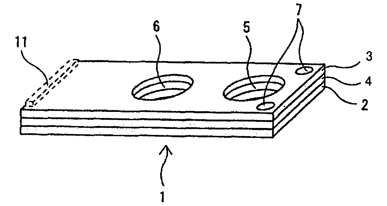
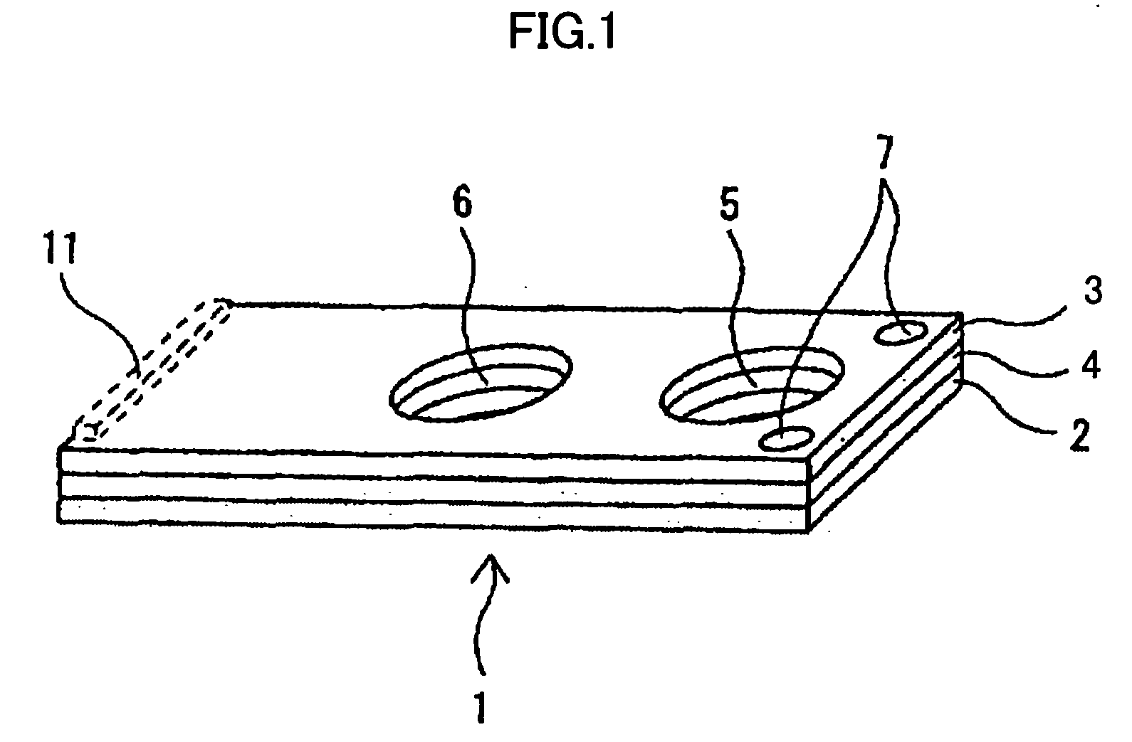
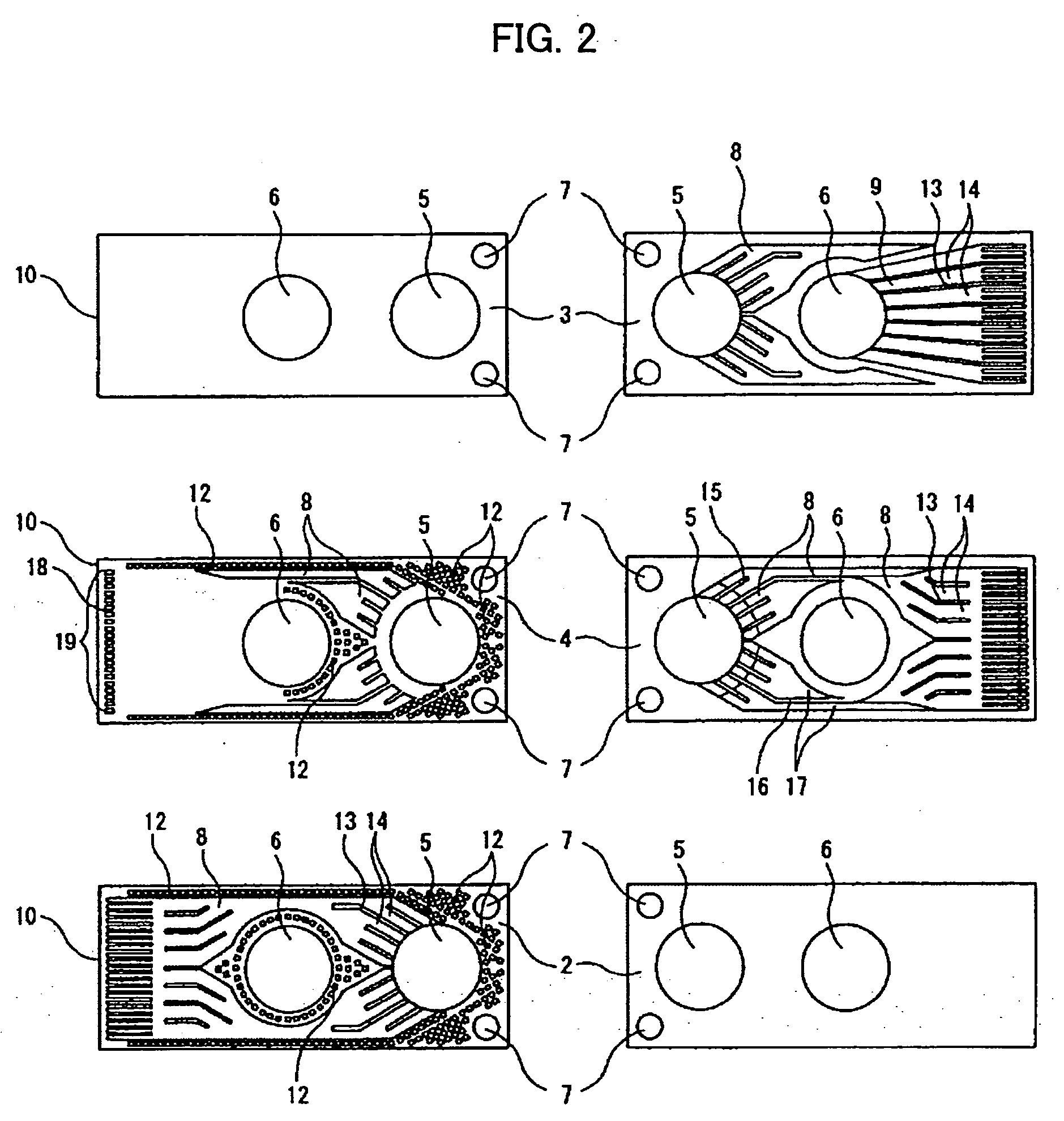
[0102]FIGS. 6 and 7 are views for explaining the present invention. A cooling device 1 of the present invention is shown in perspective view in FIG. 6, and plate members used for the cooling device 1 before they are stacked are individually shown in plan views in FIG. 7. Among these plan views, the left-hand side views show patterns formed in upper faces of the plate members, and the right-hand side views show patterns formed in lower faces (rear faces) thereof. The plate members are arranged in stacking order. As shown in FIGS. 6 and 7, in this embodiment, the cooling device is comprised of a laminate of first, second and third plate members 2, 3 and 4. The first plate member 2 disposed on one outermost side of the laminate is formed with an inlet opening 5 extending through the first plate member for introducing coolant, and an outlet opening 6 extending through the first plate member for discharging the coolant. The second plate member 3 disposed on another outermost side is prov...
PUM
 Abstract
Description
Claims
Application Information
 - Generate Ideas
- Intellectual Property
- Life Sciences
- Materials
- Tech Scout
- Unparalleled Data Quality
- Higher Quality Content
- 60% Fewer Hallucinations
Browse by: Latest US Patents, China's latest patents, Technical Efficacy Thesaurus, Application Domain, Technology Topic, Popular Technical Reports.
© 2025 PatSnap. All rights reserved.Legal|Privacy policy|Modern Slavery Act Transparency Statement|Sitemap|About US| Contact US: help@patsnap.com