Method and appratus for measurements of patterned structures
a pattern structure and measurement method technology, applied in the field of measurement techniques, can solve the problems of excluding it from continued processing, difficult to solve, bulky optical system,
- Summary
- Abstract
- Description
- Claims
- Application Information
AI Technical Summary
Benefits of technology
Problems solved by technology
Method used
Image
Examples
Embodiment Construction
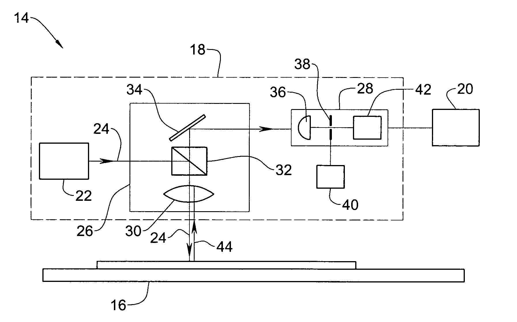
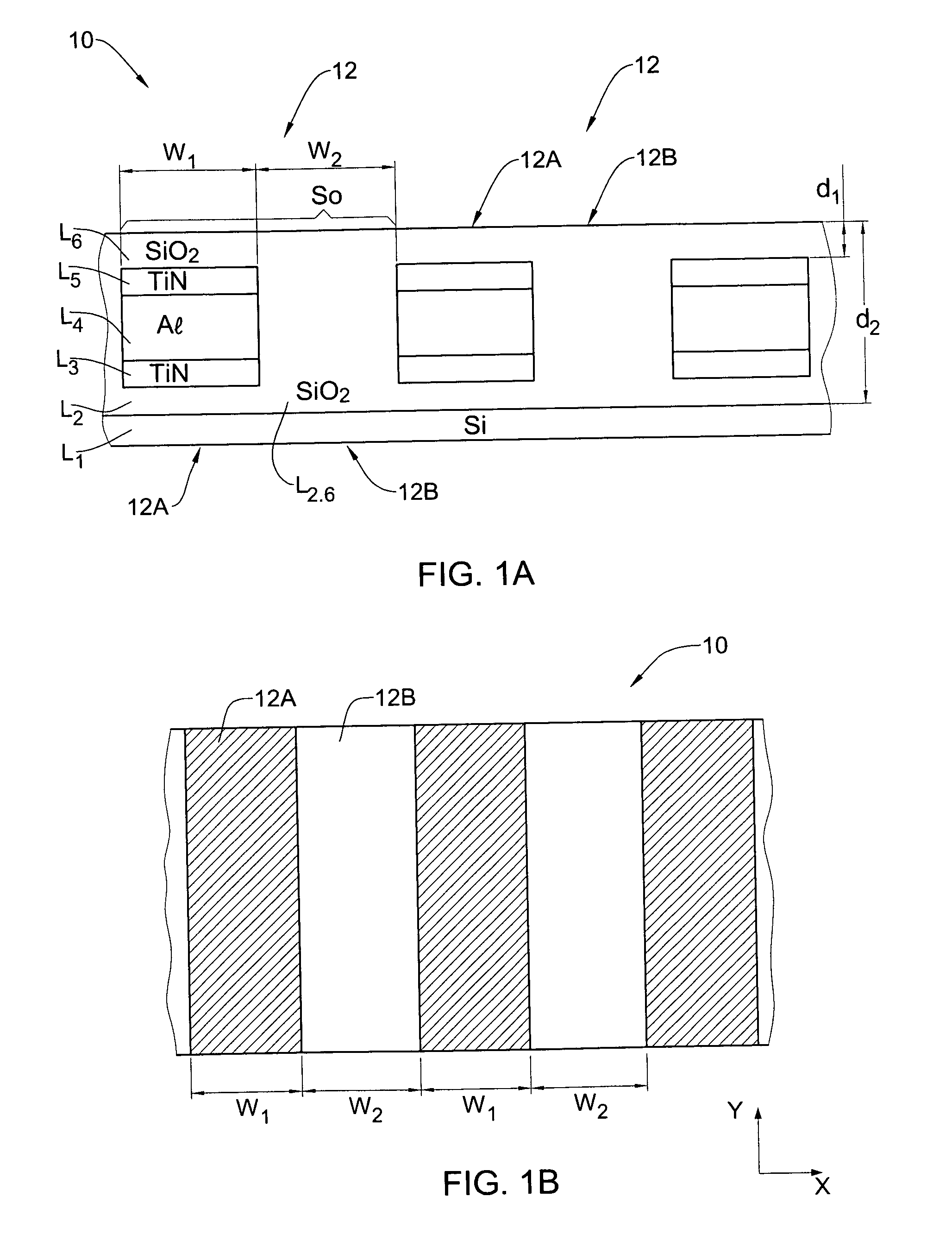
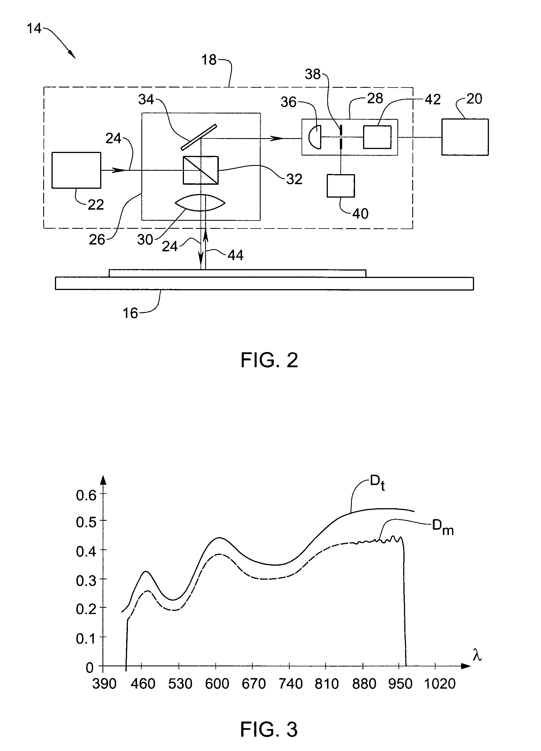
[0050] Referring to FIGS. 1a and 1b, there are partly illustrated a cross-section and a top view, respectively, of a grid-like wafer structure, generally designated 10, whose parameters are to be measured. The structure is formed of a plurality of cells, generally at 12, each constituting a grid cycle. Only three adjacent cells 12 are demonstrated in the present example with only two stacks (or elements) in each cell in order to simplify the illustration. Thus, the cell 12 comprises two stacks 12a and 12b formed of different layers. More specifically, the stack 12a includes six layers L1-L6, wherein the layers L1 and L2 and the layer L6 form two layers L1 and L2,6, respectively, of the stack 12b. As known in the conventional semiconductor devices, semiconductor structures such as sources, drains and gate electrodes, capacitors, etc. are formed in and on a semiconductor substrate (layer L1) typically made of silicon material and including metal conductors (e.g. aluminum). The substra...
PUM
 Abstract
Description
Claims
Application Information


