Process and apparatus for generating a strong phase shift optical pattern for use in an optical direct write lithography process

a technology of phase shift and lithography, which is applied in the direction of photomechanical equipment, printers, instruments, etc., can solve the problems of affecting the patterning effect of features using conventional photolithography, affecting the patterning effect of features,

Active Publication Date: 2005-07-14
BELL SEMICON LLC
View PDF2 Cites 25 Cited by
  • Summary
  • Abstract
  • Description
  • Claims
  • Application Information

AI Technical Summary

Benefits of technology

[0017] In another embodiment the invention includes a maskless lithography system. The system includes a mirror array with a plurality of movable mirrors that can operate in a piston displacement configuration and control element capable of configuring the mirrors in a desired configuration. The system includes an illumination source for directing electromagnetic waves to the mirror array to generate an exposure pattern that is projected onto a substrate. A stage is used to move the substrate facilitating the exposure of the substrate to the exposure pattern.

Problems solved by technology

As the critical dimensions for these devices grow smaller, greater difficulties will be experienced in patterning these features using conventional photolithography.
Although useful such masks suffer from a number of shortcomings.
For one, a mask set for such phase shift masks takes a long time to make.
Sometimes these mask sets can take thirty days or longer to manufacture.
Additionally, such mask sets are particularly vulnerable to defects which can have catastrophic effects on the reticle yield.
Also, due to the etch processes used in making such masks, there are numerous non-uniformities in surface conformation.
These result in unwanted and unexpected diffraction and scattering patterns which interfere with and corrupt the desired light pattern produced with these masks.
Additionally, the interactions between light and the sidewalls present in such masks create their own wave patterns which interfere with and corrupt the desired light pattern produced with these masks.
Additionally, because such phase masks require at least two exposures per layer and because many process layers are commonly used to form modern semiconductor structures, alignment difficulties between the masks and the wafer comprise significant process complications.
Additionally., imperfections in mask feature size, feature placement, phase, or transmission cannot be easily inspected and repaired.
These complications result in costs that are disproportionate to the costs involved in other aspects of the chip fabrication.
Additionally, it is a substantial effort to make small changes in the design once the masks are fabricated.
This results in additional expenditures for second, third, and even more sets of masks.
Finally, with the reduction in feature sizes, various process limitations in the conventional lithography process have made IC fabrication more difficult.
However, x-ray lithography has found only limited acceptance because of mask, source and resist technology problems.
Sources have not been sufficiently bright, and resists have not been adequately sensitive or process-resistant.
Further, x-ray masks can be complex to manufacture and current process difficulties (such as the presence of a nonzero mask to wafer gap) do not permit resolution consistent with the theoretical limits set by wavelength.
For at least these reasons, x-ray lithography has not gained widespread acceptance.
Unfortunately, the imaging step of e-beam lithography is relatively slow.
This combination of raster scanning and multiple passes requires a long time to produce a pattern image.
Thus, e-beam lithography fabrication processes have a relatively low throughput.
As critical dimensions decrease these problems and the costs inherent in solving them will only increase.

Method used


Image

  • Process and apparatus for generating a strong phase shift optical pattern for use in an optical direct write lithography process
  • Process and apparatus for generating a strong phase shift optical pattern for use in an optical direct write lithography process
  • Process and apparatus for generating a strong phase shift optical pattern for use in an optical direct write lithography process

Examples


Embodiment Construction

[0033] The present invention has been particularly shown and described with respect to certain embodiments and specific features thereof. The embodiments set forth hereinbelow are to be taken as illustrative rather than limiting. It should be readily apparent to those of ordinary skill in the art that various changes and modifications in form and detail may be made without departing from the spirit and scope of the invention.

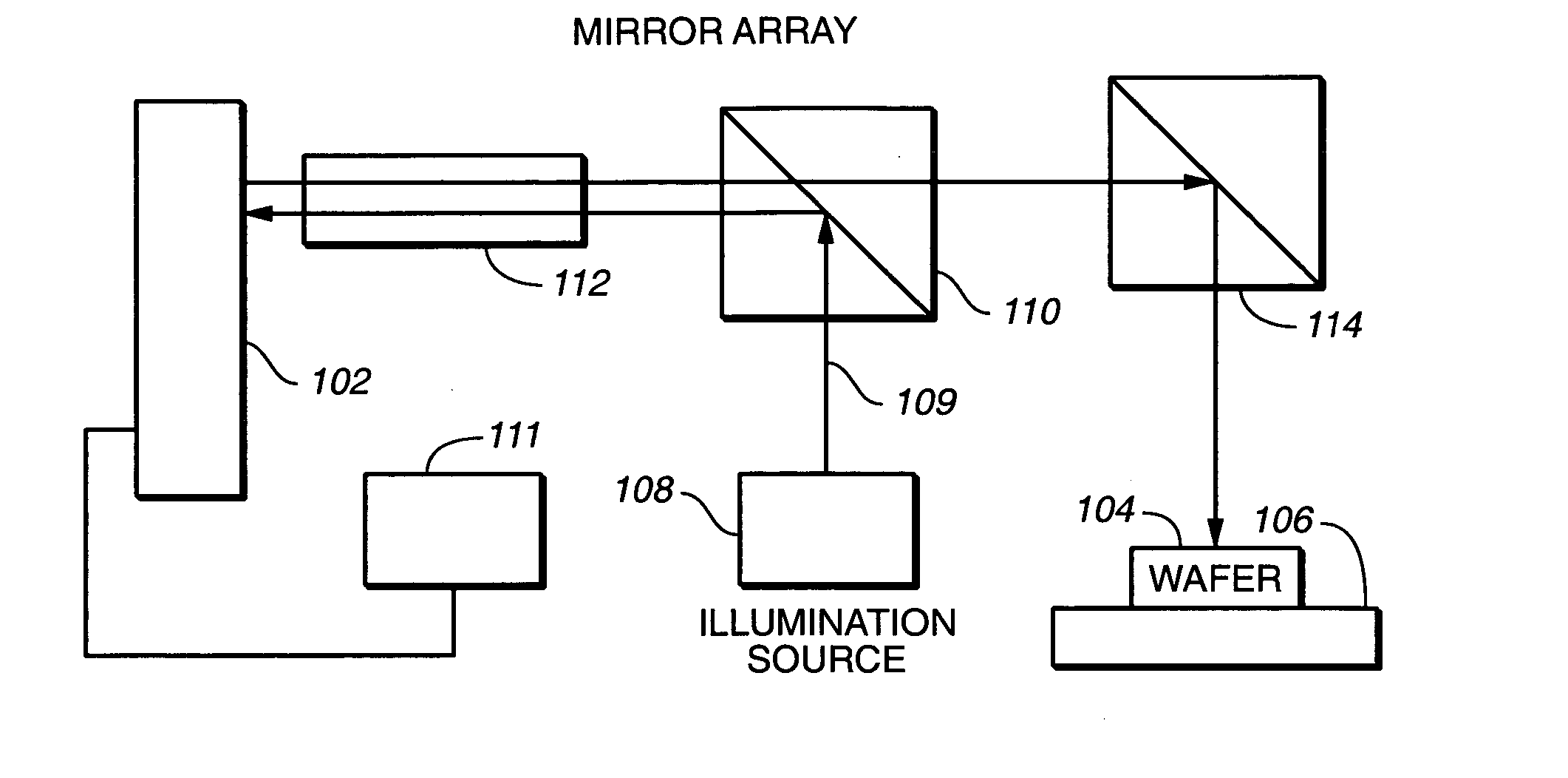
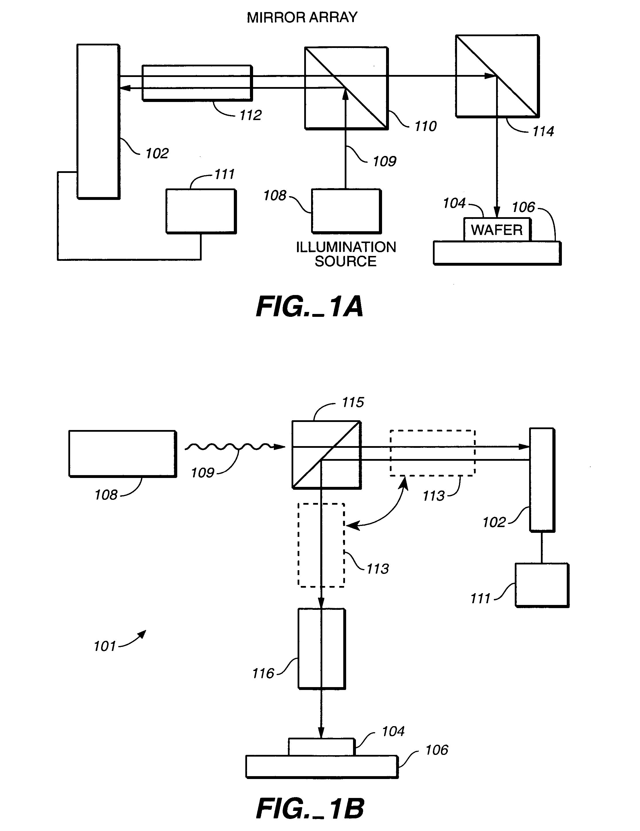
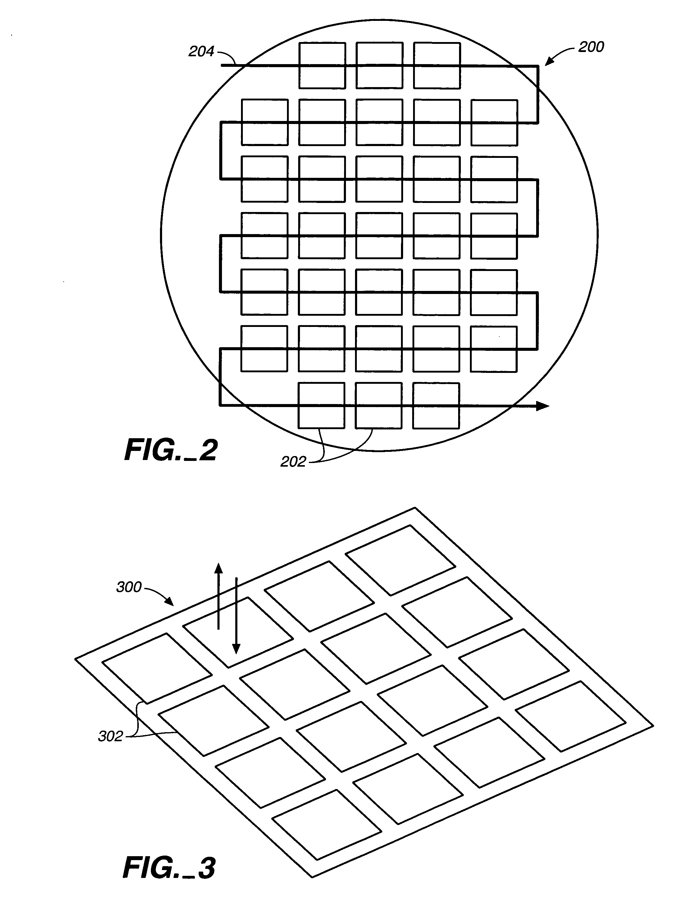
[0034] In the following detailed description, fabrication methods and apparatus for implementing direct write optical lithography systems is set forth. Such systems and methods use programmable optical mirrors in a maskless lithography system to form desired optical patterns on a substrate. The maskless direct-write lithography system provided uses an array of mirrors configured to operate in a torsional (i.e., tilted) mode, a piston-displacement (“piston”) mode, or capable of operating in both modes. A scanning apparatus is provided that uses the mirror array ...


PUM

PropertyMeasurementUnit
widthaaaaaaaaaa
widthaaaaaaaaaa
widthaaaaaaaaaa

Abstract

The present invention provides methods and apparatus for accomplishing a strong phase shift direct write lithography process using reconfigurable optical mirrors. A maskless lithography system is provided. The maskless direct-write lithography system provided uses an array of mirrors configured to operate in a tilting mode, a piston-displacement mode, or both in combination. The controlled mirror array is used to generate strong phase shift optical patterns which are directed onto a photoimageable layer of a substrate in order to facilitate pattern transfer. In order to avoid constraining the system to forming edges of patterns aligned with the array of mirrors, gray-scale techniques are used for subpixel feature placement.

Description

CROSS-REFERENCE TO RELATED APPLICATIONS [0001] This application claims priority of U.S. Provisional Patent Application No. 60 / 513,780 (Attorney DocketNo. 03-1810), filed 22 Oct. 2003, which application is incorporated herein by reference in its entirety for all purposes. [0002] This application also claims priority of U.S. Provisional Patent Application No. 60 / 535,586, filed 1 Jan. 2004, which application is incorporated herein by reference in its entirety for all purposes. [0003] This application also claims priority of U.S. Utility Patent Application Ser. No. 10 / 825,342 (Attorney Docket No. 03-1810 / LSI1P239), filed 14 Apr. 2004, which application is incorporated herein by reference in its entirety for all purposes.FIELD OF THE INVENTION [0004] The present invention relates to methods and apparatus for forming patterns on substrate surfaces. More particularly, the present invention relates to methods for directly writing patterns onto a wafer to create semiconductor devices on the ...

Claims


Application Information

Patent Timeline
Patent Type & Authority Applications(United States)
IPC IPC(8): G03F7/00G03F7/20
CPCG03F7/70291
Inventor EIB, NICHOLAS K.CROFFLE, EBO H.CALLAN, NEAL P.
Owner BELL SEMICON LLC
Why Eureka
Try Eureka