Optical element, lithographic apparatus comprising such optical element and device manufacturing method

a technology of optical elements and lithographic apparatuses, which is applied in the direction of stone-like material working apparatuses, printers, projectors, etc., can solve the problems of high thermal stress and cracking, unwanted exposure of resists, sublimation and oxidation in high power levels, etc., and achieve the effect of reducing or eliminating radiations and reducing radiation intensity

Inactive Publication Date: 2005-07-21
ASML NETHERLANDS BV
View PDF6 Cites 8 Cited by
  • Summary
  • Abstract
  • Description
  • Claims
  • Application Information

AI Technical Summary

Benefits of technology

[0009] It is therefore an aspect of the invention to provide an alternative optical element that enables substantial transmission or reflection, or both transmission and reflection, of radiations with desired wavelengths (like e.g. EUV) and substantially reduces or eliminates radiations with undesired wavelengths (like e.g. radiations selected from the group consisiting of one or more of VUV, DUV, UV, VIS, and IR radiation). It is a further aspect of the inventio

Problems solved by technology

These unwanted frequencies will propagate and cause heating problems in the illumination and projection systems and cause unwanted exposure of the resist if not blocked.
However, such a film is very delicate and becomes very hot, 200-300° C. or more, leading to high thermal stresses and cracking, sublimation and oxidation in the high power l

Method used


Image

  • Optical element, lithographic apparatus comprising such optical element and device manufacturing method
  • Optical element, lithographic apparatus comprising such optical element and device manufacturing method
  • Optical element, lithographic apparatus comprising such optical element and device manufacturing method

Examples


Embodiment Construction

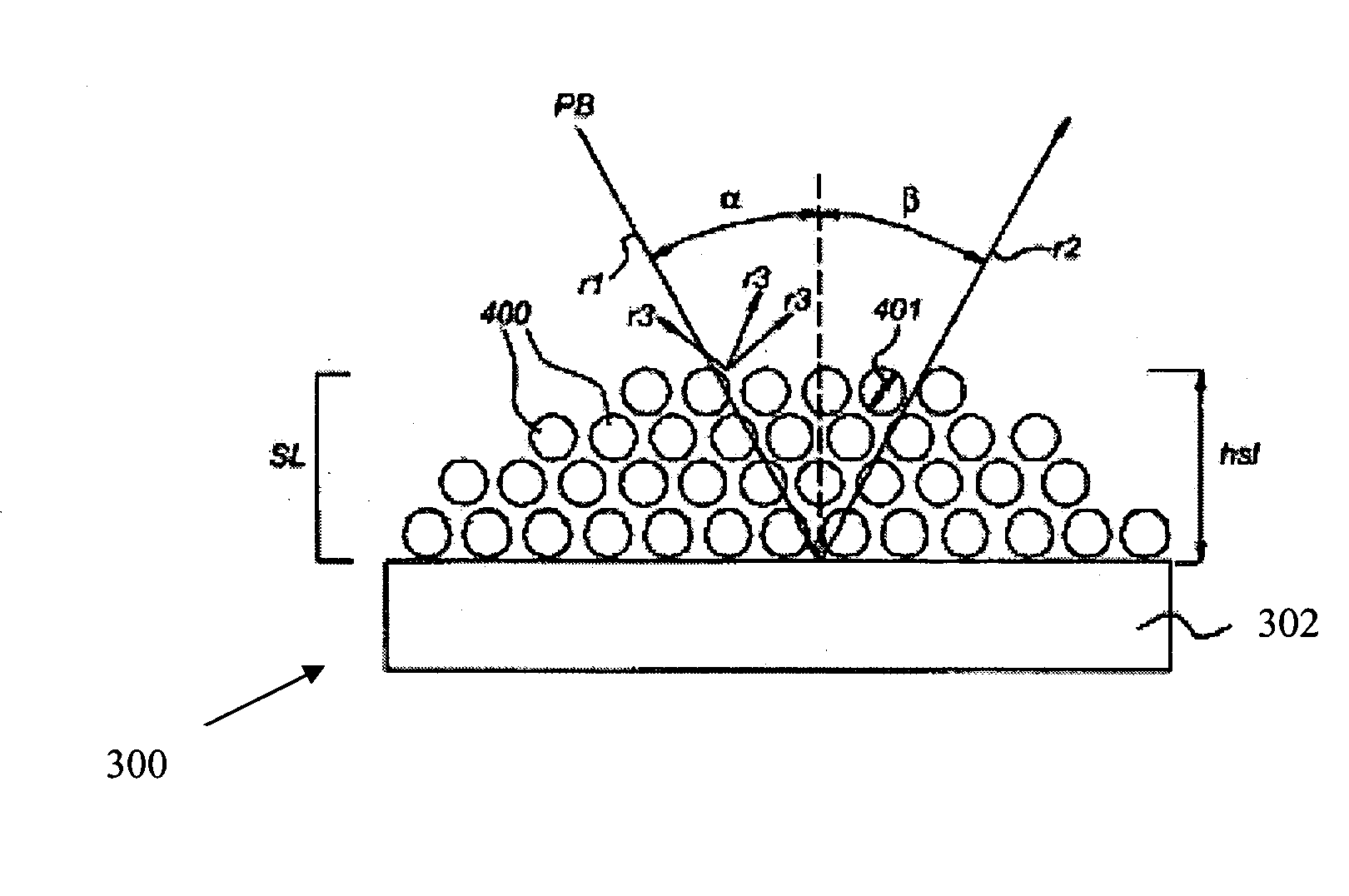
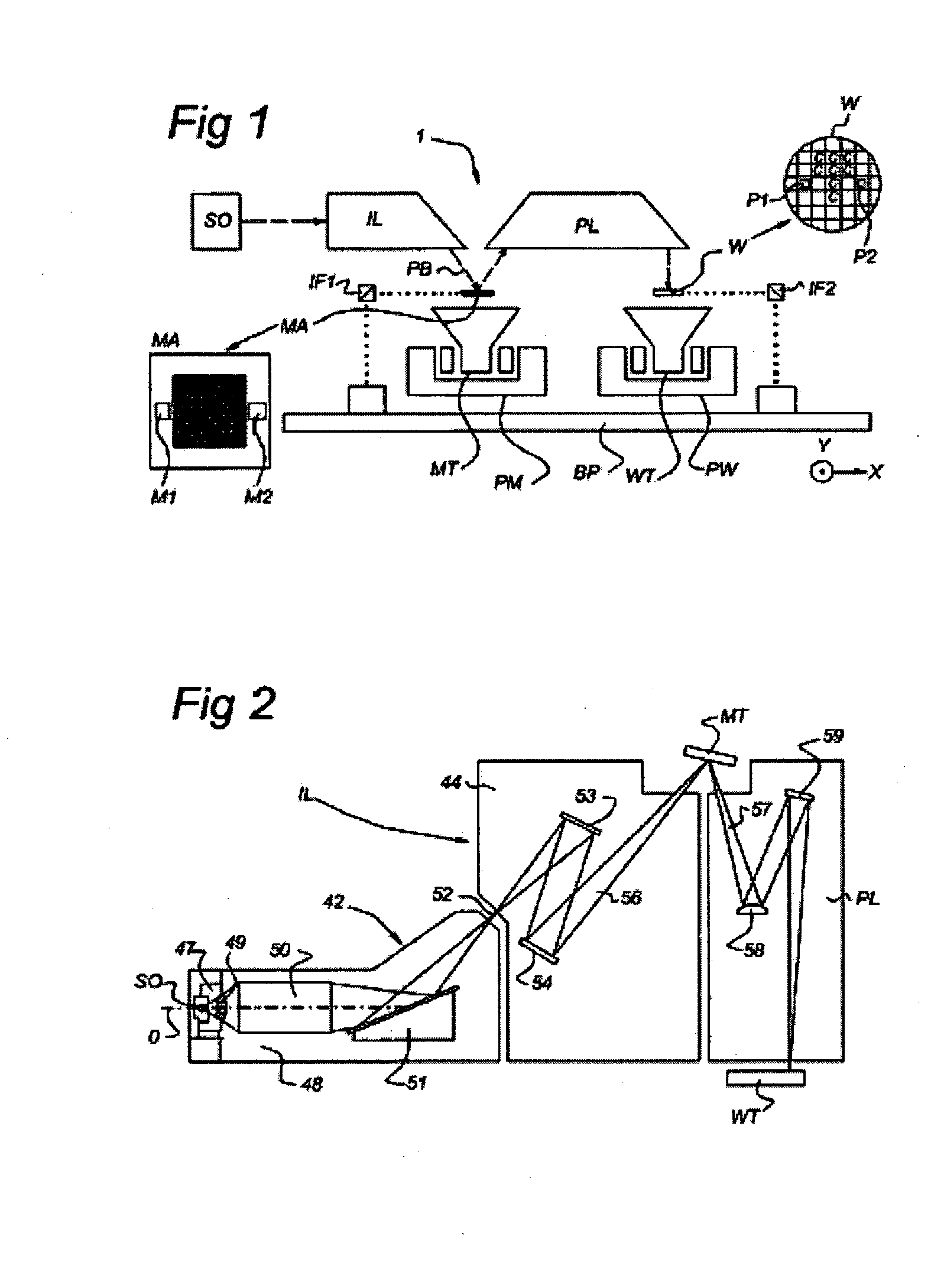
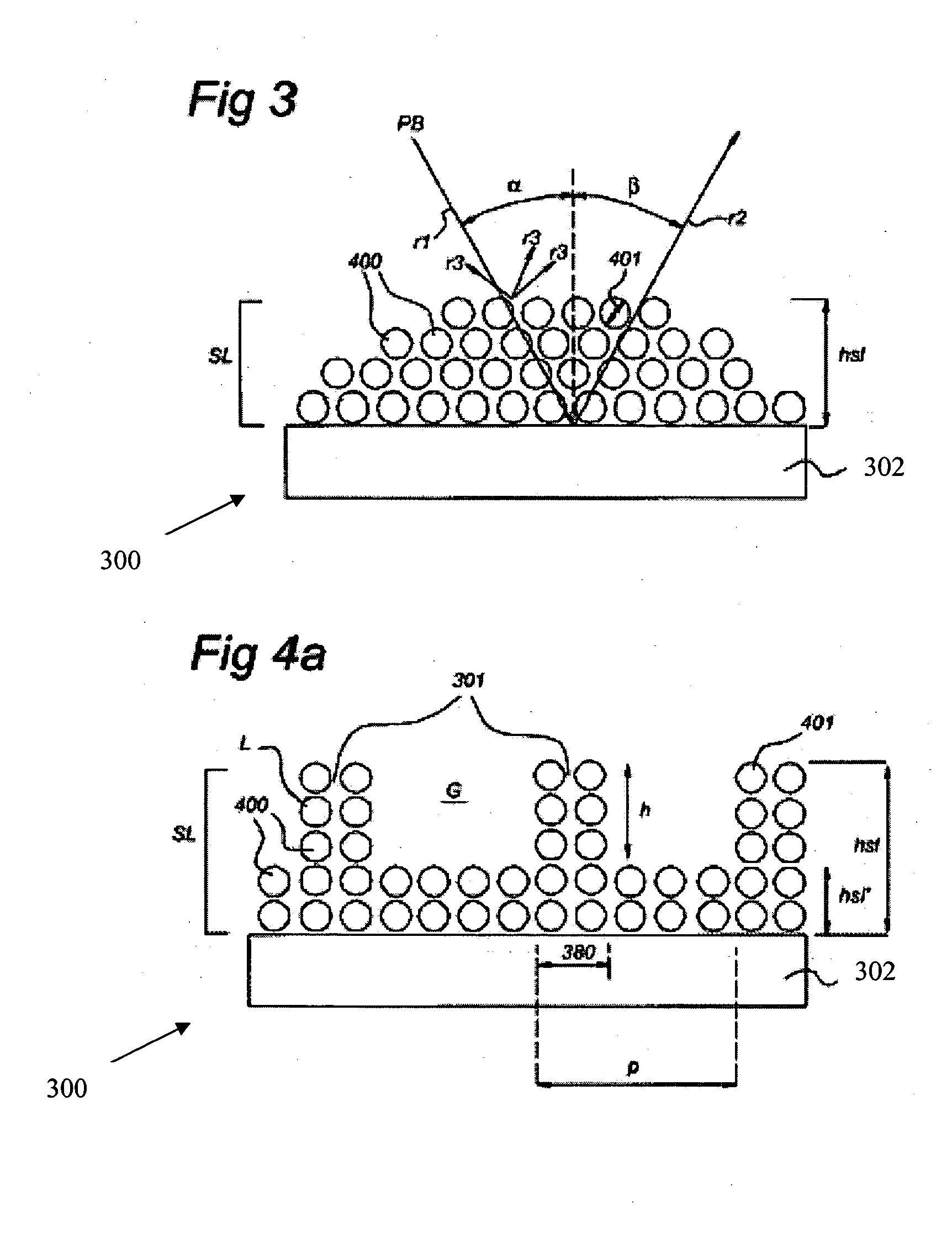
[0052]FIG. 1 schematically depicts a lithographic apparatus according to a particular embodiment of the invention. The apparatus includes an illumination system (illuminator) IL configured to provide a projection beam PB of radiation (e.g. UV or EUV radiation). A first support structure (e.g. a mask table) MT is configured to support a patterning structure (e.g. a mask) MA and is connected to a first positioning device PM that accurately positions the patterning structure with respect to a projection system (“lens”) PL. A substrate table (e.g. a wafer table) WT is configured to hold a substrate (e.g. a resist-coated wafer) W and is connected to second positioning device PW that accurately positions the substrate with respect to the projection system PL. The projection system (e.g. a reflective projection lens) PL images a pattern imparted to the projection beam PB by the patterning structure MA onto a target portion C (e.g. including one or more dies) of the substrate W.

[0053] As h...


PUM

PropertyMeasurementUnit
Thicknessaaaaaaaaaa
Thicknessaaaaaaaaaa
Thicknessaaaaaaaaaa

Abstract

An optical element includes a substrate having at least one surface on which a layer of material is disposed, the layer of material being selected to be at least partially transmissive to radiation with a predetermined wavelength λ. The surface of material includes particles having a diameter in a range of 1-500 nm and the layer of material has a layer thickness in the range of 10-2000 nm. Undesired radiations, e.g. UV and DUV radiations, are substantially reduced or eliminated by scattering, e.g. Mie scattering and/or Raleigh scattering, and/or by absorption by the particles while desired radiations are transmitted to the surface of the optical element.

Description

BACKGROUND OF THE INVENTION [0001] 1. Field of the Invention [0002] This invention relates to an optical element, a lithographic apparatus comprising such optical element and to a device manufacturing method. [0003] 2. BRIEF DESCRIPTION OF RELATED ART [0004] A lithographic apparatus is a machine that applies a desired pattern onto a target portion of a substrate. Lithographic apparatus can be used, for example, in the manufacture of integrated circuits (ICs). In that circumstance, a patterning structure, such as a mask, may be used to generate a circuit pattern corresponding to an individual layer of the IC, and this pattern can be imaged onto a target portion (e.g. comprising part of, one or several dies) on a substrate (e.g. a silicon wafer) that has a layer of radiation-sensitive material (resist). In general, a single substrate will contain a network of adjacent target portions that are successively exposed. Known lithographic apparatus include so-called steppers, in which each ...

Claims


Application Information

Patent Timeline
IPC IPC(8): G02B1/00G21K1/06G02B1/10G02B5/18G02B5/28G03F7/20G21K5/02H01L21/027
CPCG02B1/00G02B1/10G02B5/18G03F7/70958G03F7/70308G03F7/70575G03F7/70191B28D1/086B28D1/127
Inventor BAKKER, LEVINUS PIETER
Owner ASML NETHERLANDS BV
Why Eureka
Try Eureka