Method for forming a junction region of a semiconductor device

a semiconductor device and junction region technology, applied in the direction of semiconductor devices, basic electric elements, electrical appliances, etc., can solve the problems of shrinkage of devices, difficulty in forming ultra shallow junctions, and increased leakage current in p-n junctions, so as to reduce the damage to the wafer substrate, the effect of not being damaged

Active Publication Date: 2005-07-28
UNITED MICROELECTRONICS CORP
View PDF2 Cites 9 Cited by
  • Summary
  • Abstract
  • Description
  • Claims
  • Application Information

AI Technical Summary

Benefits of technology

[0009] Another objective of the present invention is to provide a method for forming a junction region of a semiconductor device by employing carbon-containing plasma treatment, herein carbon-containing plasma treatment produces carbon ions to pene

Problems solved by technology

With advances in semiconductor technology, the dimensions of the integrated circuit (IC) devices have shrunk to the deep sub-micron region, some problems are incurred due to the process of scaling down.
Consequently, it is difficult to form ultra shallow junctio

Method used


Image

  • Method for forming a junction region of a semiconductor device
  • Method for forming a junction region of a semiconductor device
  • Method for forming a junction region of a semiconductor device

Examples


Embodiment Construction

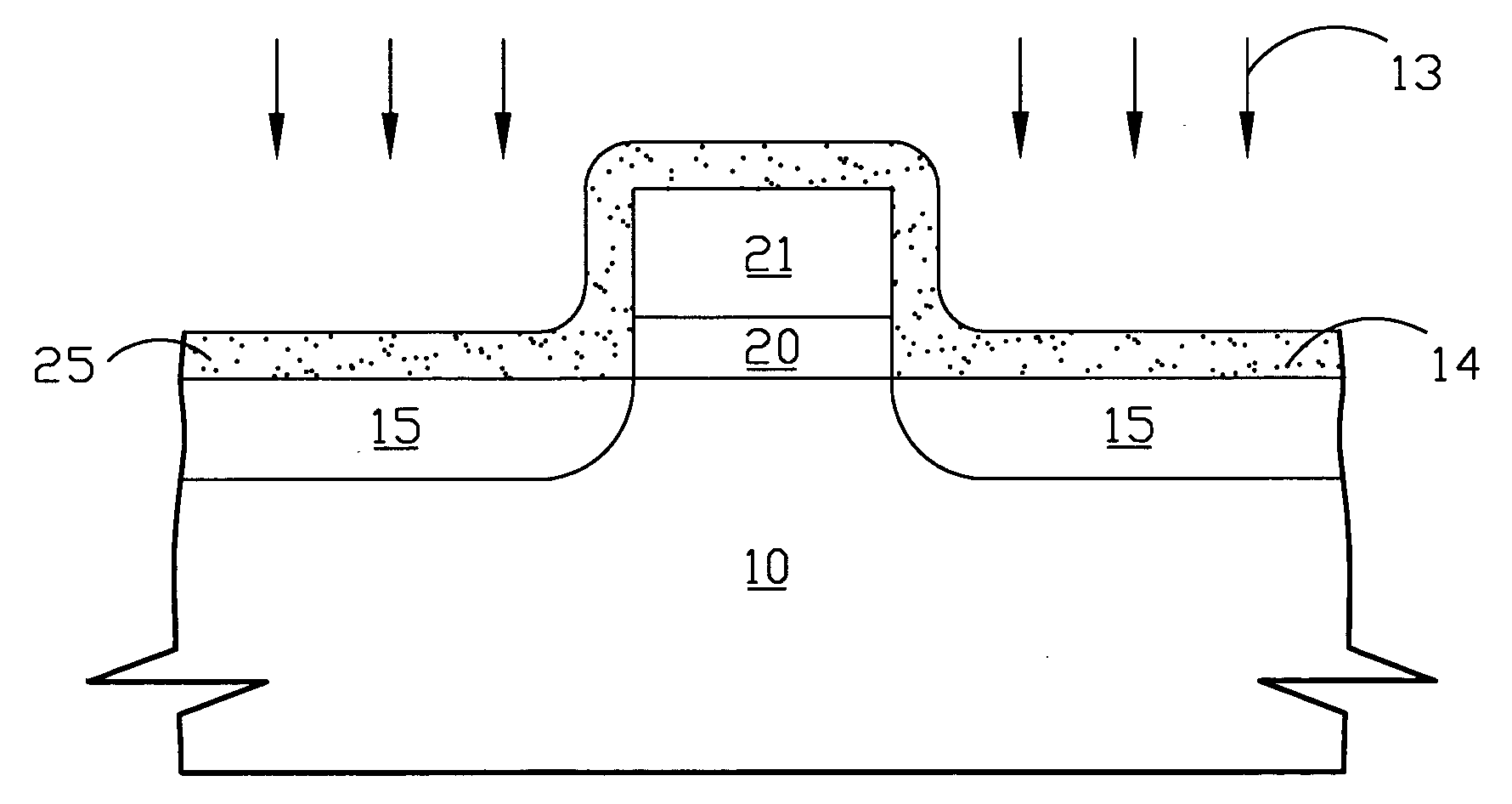
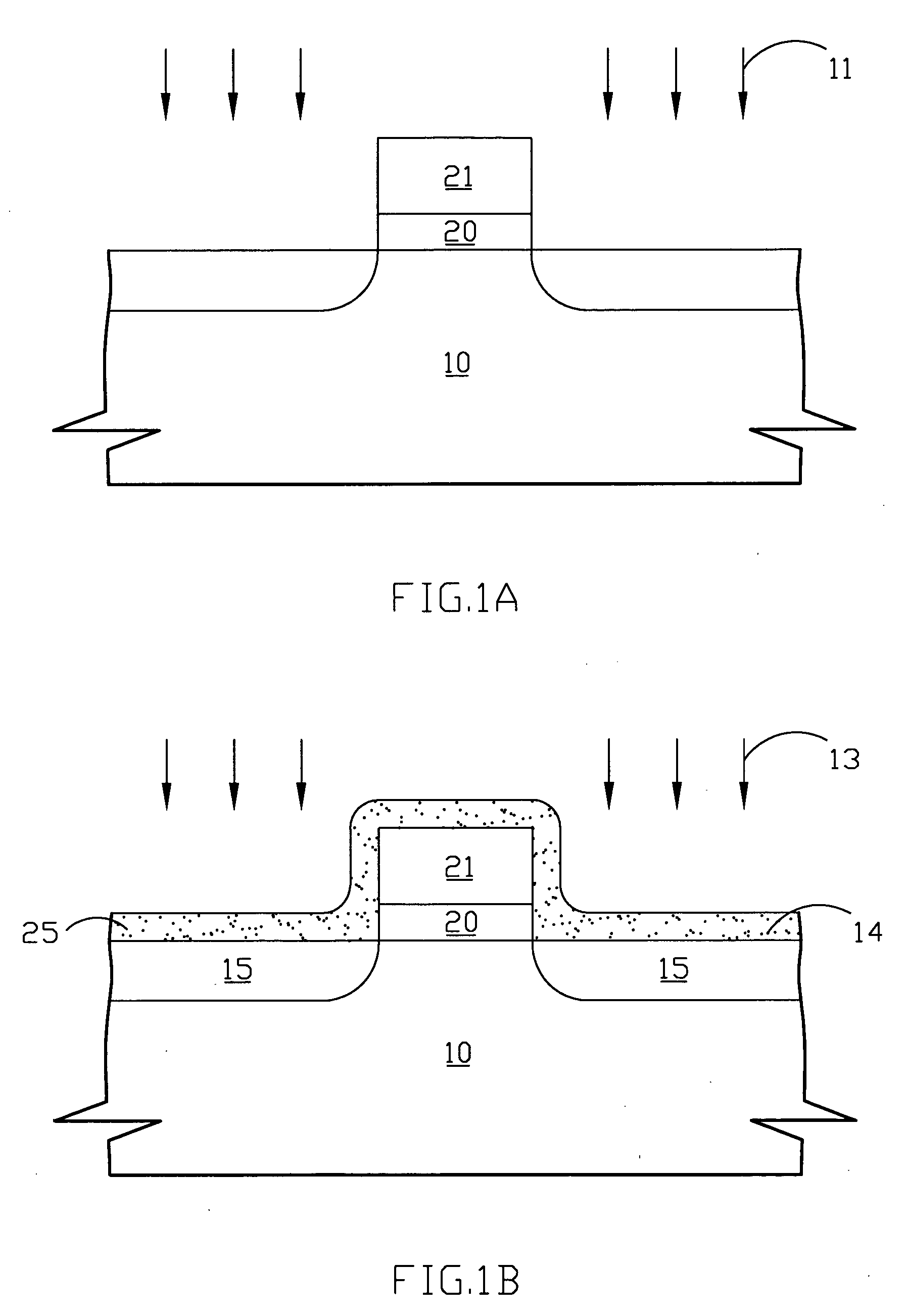
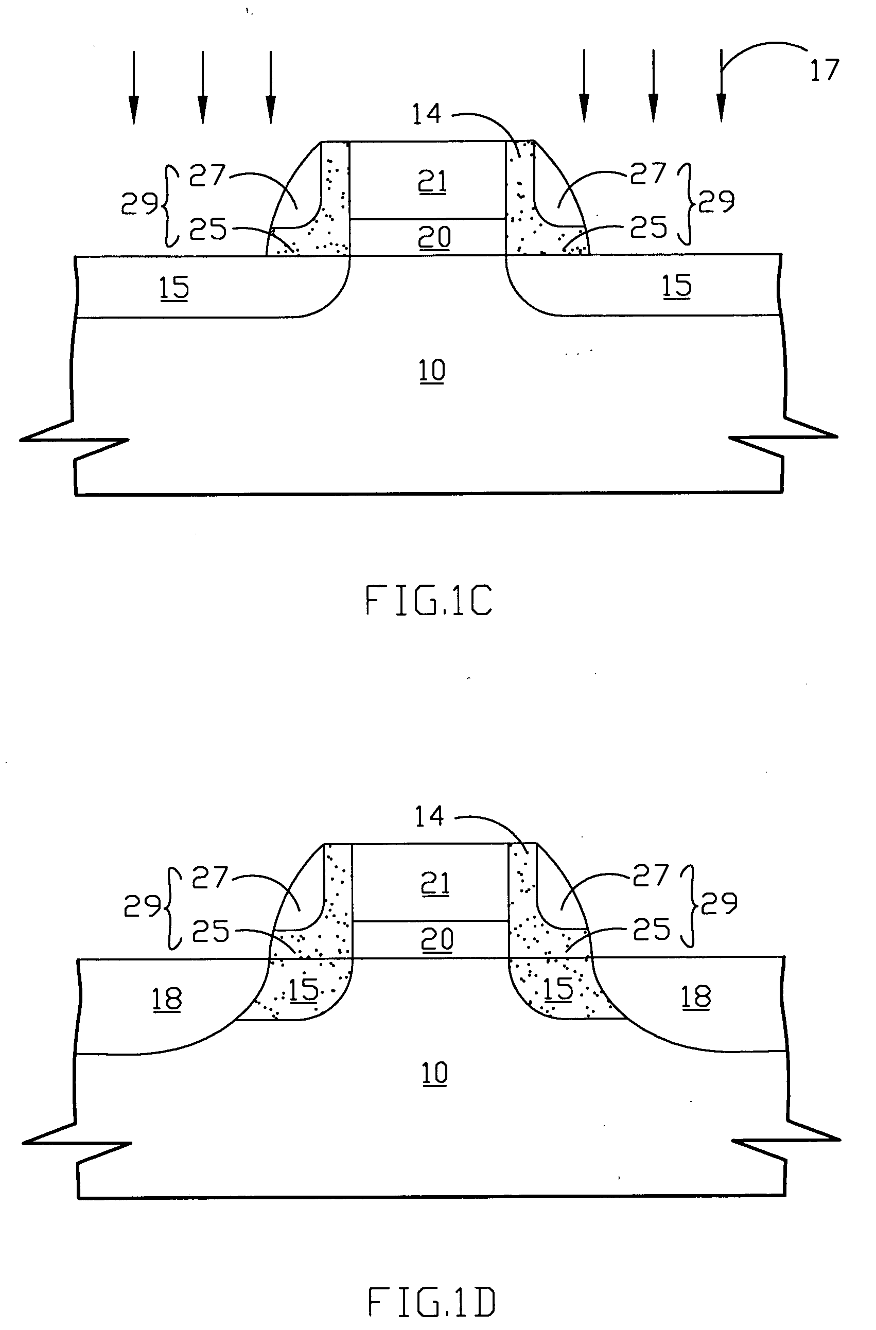
[0013] There is shown a representative portion of a semiconductor structure of the present invention in enlarged, cross-sections of the two dimensional views at several stages of fabrication. The drawings are not necessarily to scale, as the thickness of the various layers are shown for clarify of illustration and should not be interpreted in a limiting sense. Accordingly, these regions will have dimensions, including length, width and depth, when fabricated in an actual device.

[0014] A method for forming a junction region of a semiconductor device is disclosed. The steps of the method include providing a semiconductor substrate. A gate structure is formed on the semiconductor substrate. A dopant is implanted into the semiconductor substrate to form the junction region. An insulator layer is formed on the gate structure and the semiconductor substrate. A carbon-containing plasma treatment is performed to the insulator layer. A spacer is formed on a side-wall of the gate structure a...


PUM


Abstract

A method for forming a junction region of a semiconductor device is disclosed. The steps of the method include providing a semiconductor substrate. A gate structure is formed on the semiconductor substrate. A dopant is implanted into the semiconductor substrate to form the junction region. An insulator layer is formed on the gate structure and the semiconductor substrate. A carbon-containing plasma treatment is performed to the insulator layer. A spacer is formed on a side-wall of the gate structure and the dopant is implanted into the semiconductor substrate to form a source/drain region next to the junction region. A heat treatment is performed to the semiconductor substrate.

Description

BACKGROUND OF THE INVENTION [0001] 1. Field of the Invention [0002] The invention relatives to a method for forming a junction region of a semiconductor device, more particularly to the method for forming a junction region of a PMOS semiconductor device. [0003] 2. Description of the Prior Art [0004] As semiconductor devices, such as complementary metal-oxide-semiconductor devices, become highly integrated, the area occupied by the devices shrinks, as well as the design rule. With advances in semiconductor technology, the dimensions of the integrated circuit (IC) devices have shrunk to the deep sub-micron region, some problems are incurred due to the process of scaling down. [0005] With the progress of semiconductor elements, the manufacturing of semiconductor elements is more and more precise and therefore, the depth distribution of impurity atoms is more and more precise. In generally, an ion implanting method is used to precisely control the depth and concentration distributions o...

Claims


Application Information

Patent Timeline
IPC IPC(8): H01L21/225H01L21/28H01L21/336H01L21/4763H01L29/49H01L29/78
CPCH01L21/2256H01L21/28176H01L29/7833H01L29/665H01L29/6656H01L29/4983
Inventor CHEN, YU-KUNYANG, NENG-HUICHIEN, CHIN-CHENGWANG, HSIANG-YING
Owner UNITED MICROELECTRONICS CORP
Why Eureka
Try Eureka