

High voltage switching devices and process for forming same
- Summary
- Abstract
- Description
- Claims
- Application Information
AI Technical Summary
Benefits of technology
Problems solved by technology
Method used
Image

Examples
Embodiment Construction
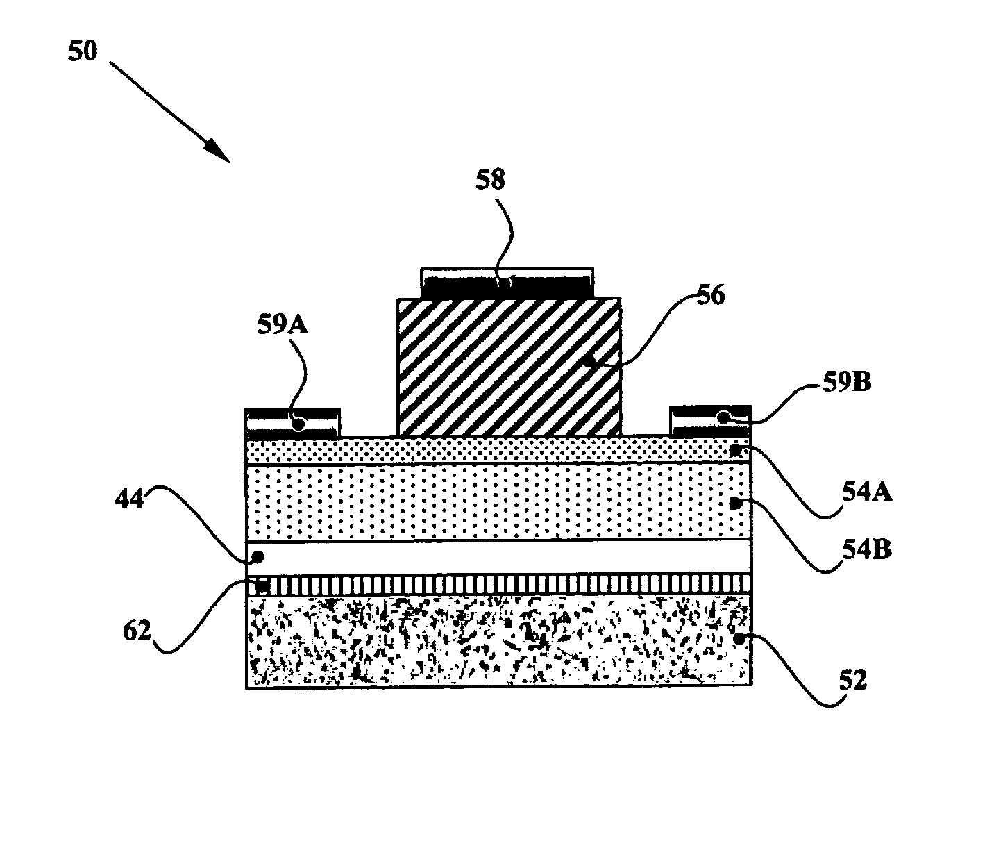
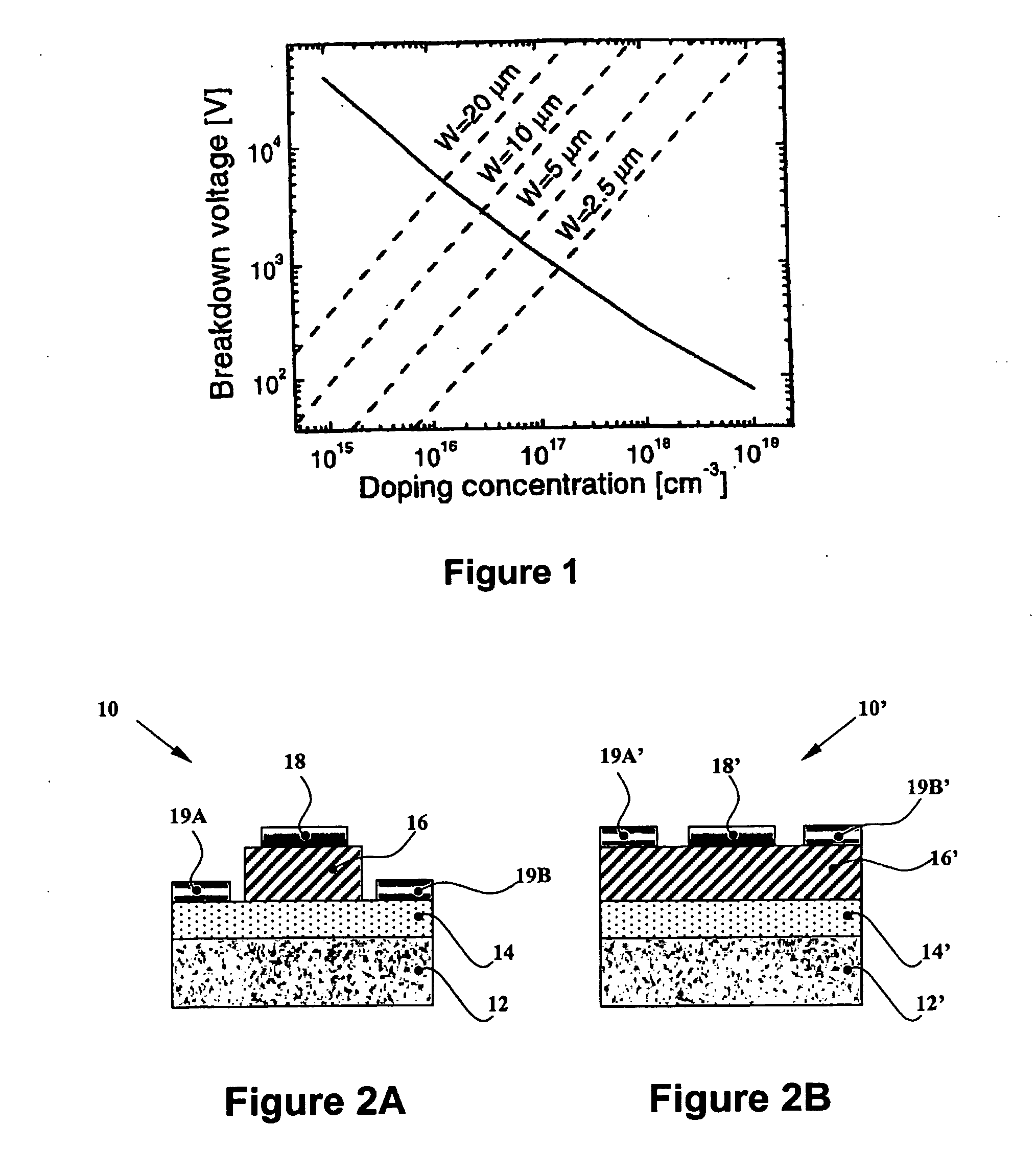
[0067] For fabricating microelectronic switching devices of relatively low breakdown voltages (i.e., <2 kV), thin GaN layers can be directly deposited by MOVPE on the foreign substrate, such as sapphire, Si, and SiC. Despite the fact that such directly deposited GaN layers are relatively thin (i.e., <10 μm), strain in the GaN layer caused by thermal expansion differences between the foreign substrate and the GaN layers results in significant cracking, pitting and defect productionIt is therefore difficult to deposit low-doped GaN layers of this thickness (i.e., <10 μm) on top of thin, conductive GaN layers on foreign substrates for fabricating Schottky rectifiers having breakdown voltages lower than about 2 kV. The following innovative and preferred embodiments address these limitations;
Conductive GaN Base Layer Formed Over One or More Interfacial Layers by MOVPE
[0068] The present invention provides a conductive GaN base layer of n-type conductivity, which is formed over a foreig...
PUM
 Abstract
Description
Claims
Application Information