Semiconductor photodetector and its production method

a technology of semiconductor photodetectors and production methods, applied in the field of semiconductor photodetectors, can solve the problems of reducing the yield and reproducibility of semiconductor photodetectors, requiring a complicated and hard process, and disconnection or insulation failure, so as to reduce the projection of semiconductor layers, prevent a projection in the surface portion, and reduce the effect of semiconductor layer climbing

Inactive Publication Date: 2005-08-11
HAMAMATSU PHOTONICS KK
View PDF29 Cites 19 Cited by
  • Summary
  • Abstract
  • Description
  • Claims
  • Application Information

AI Technical Summary

Benefits of technology

[0006] The present invention has been accomplished under the above circumstances and an object of the invention is therefore to realize easy fabrication of a semiconductor photodetector with improvement in yield and reproducibility.
[0008] The semiconductor photodetector having the above configuration is of the structure in which at least a portion of the top surface portion (surface) of the first semiconductor layer makes a flat surface at the height equal to that of the middle step surface of the semi-insulating substrate and in which the top surface portion (surface) of the second semiconductor layer makes a flat surface at the height equal to that of the upper step surface of the semi-insulating substrate. Therefore, each of the electrodes in contact with the respective semiconductor layers can be placed on a continuous flat surface. As a result, it becomes feasible to provide the semiconductor photodetector less likely to suffer disconnection and insulation failure, as compared with those wherein the electrodes are placed astride the ramp portion.
[0009] When further comprising a third semiconductor layer formed between the first semiconductor layer and the second semiconductor layer and having a carrier density lower than that of the first semiconductor layer or the second semiconductor layer, the semiconductor photodetector can be constructed with the third semiconductor layer as a light absorbing layer. In this case, when the third semiconductor layer is set in an optimal thickness for a length of optical absorption determined by a wavelength of incident light, the semiconductor photodetector can be constructed with high optical absorption efficiency.
[0012] According to the above production method, level differences are made in the semi-insulating substrate itself, whereby the semiconductor photodetector with the electrodes on the flat surfaces of the semi-insulating substrate less likely to suffer disconnection can be readily fabricated without use of the special etching technique. As a result, it is feasible to provide the semiconductor photodetector excellent in yield and reproducibility.
[0014] Furthermore, in order to minimize the projection of the semiconductor layer in the surface portion, preferably, the first step is to form the recess of the semi-insulating substrate so that at least a side wall portion on the second electrode side among side wall portions in a sectional shape along a direction connecting the first electrode to the second electrode is of an inverted mesa shape (a shape of the recess the side wall portion of which is inclined in the radial direction of the bottom surface of the recess). Since each semiconductor layer is formed according to the shape of the recess, when the recess is formed in this sectional shape, it is feasible to decrease the climbing of the semiconductor layers near the ramp portion in their deposition steps and to prevent a projection in the surface portion. As a result, electrode wiring can be provided on a flatter surface, which can improve the yield and reproducibility of the semiconductor photodetector more.
[0015] As long as at least the side wall portion on the second electrode side is formed in the inverted mesa shape in the sectional shape of the recess, even if the side wall portion on the first electrode side is formed in the normal mesa shape, the aforementioned effect can also be achieved by further etching the semi-insulating substrate in that part.

Problems solved by technology

Providing electrode wiring on such ramp part can cause disconnection or insulation failure due to deterioration of coverage, and also requires a complicated and hard process.
As a result, there were such problems as degradation of yield and reproducibility of semiconductor photodetectors fabricated, degradation of reliability as a product, and so on.

Method used


Image

  • Semiconductor photodetector and its production method
  • Semiconductor photodetector and its production method
  • Semiconductor photodetector and its production method

Examples


first embodiment

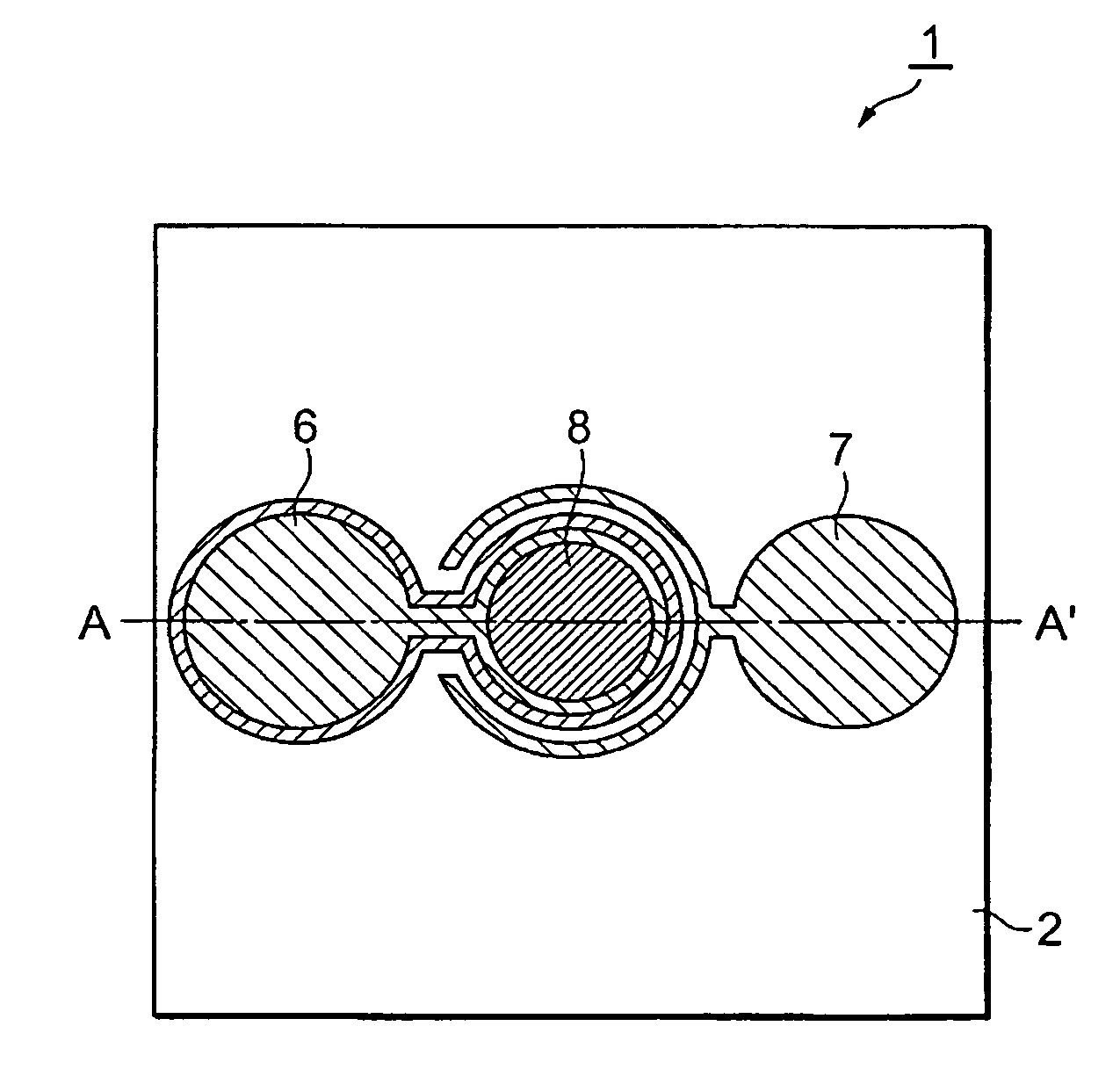
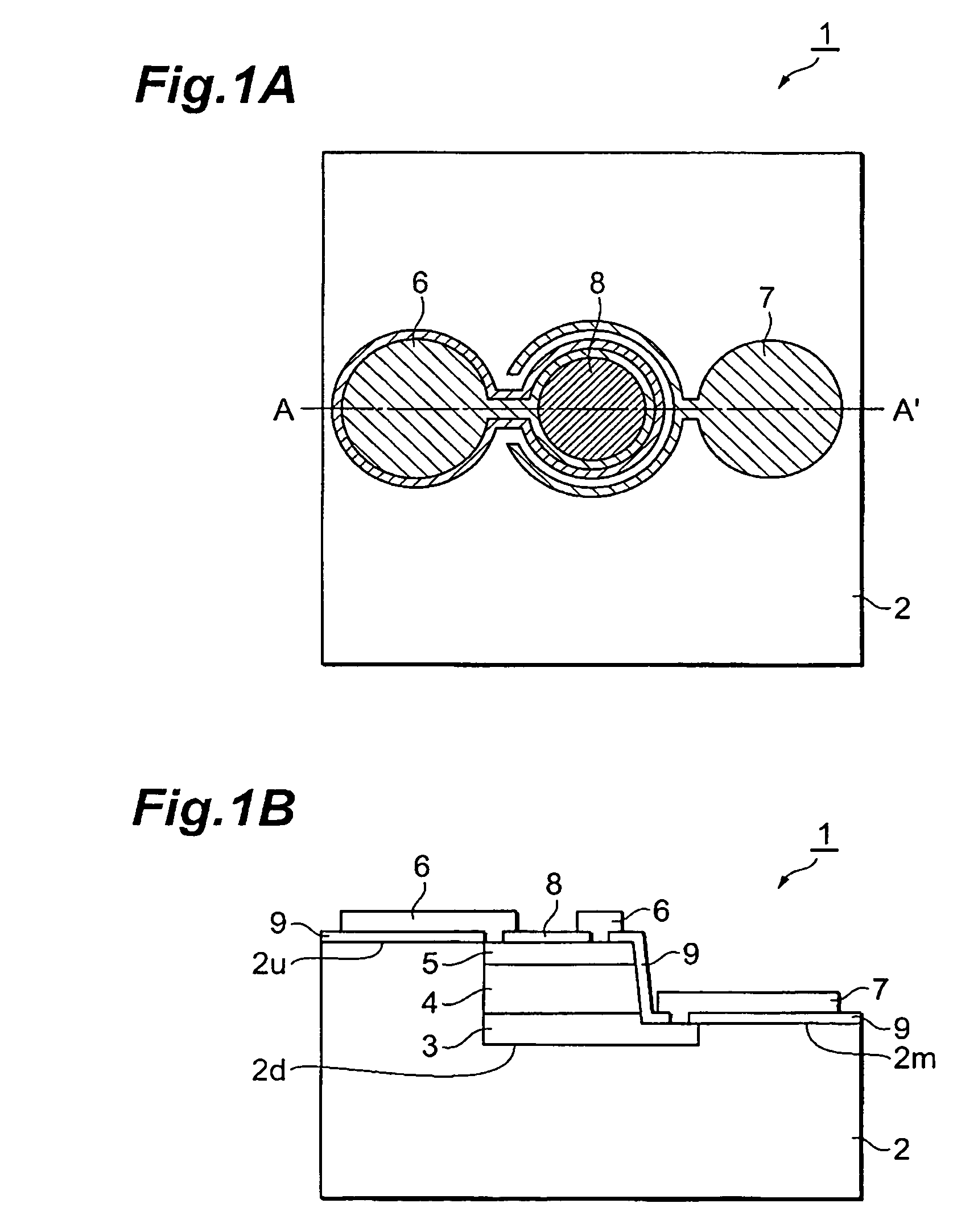
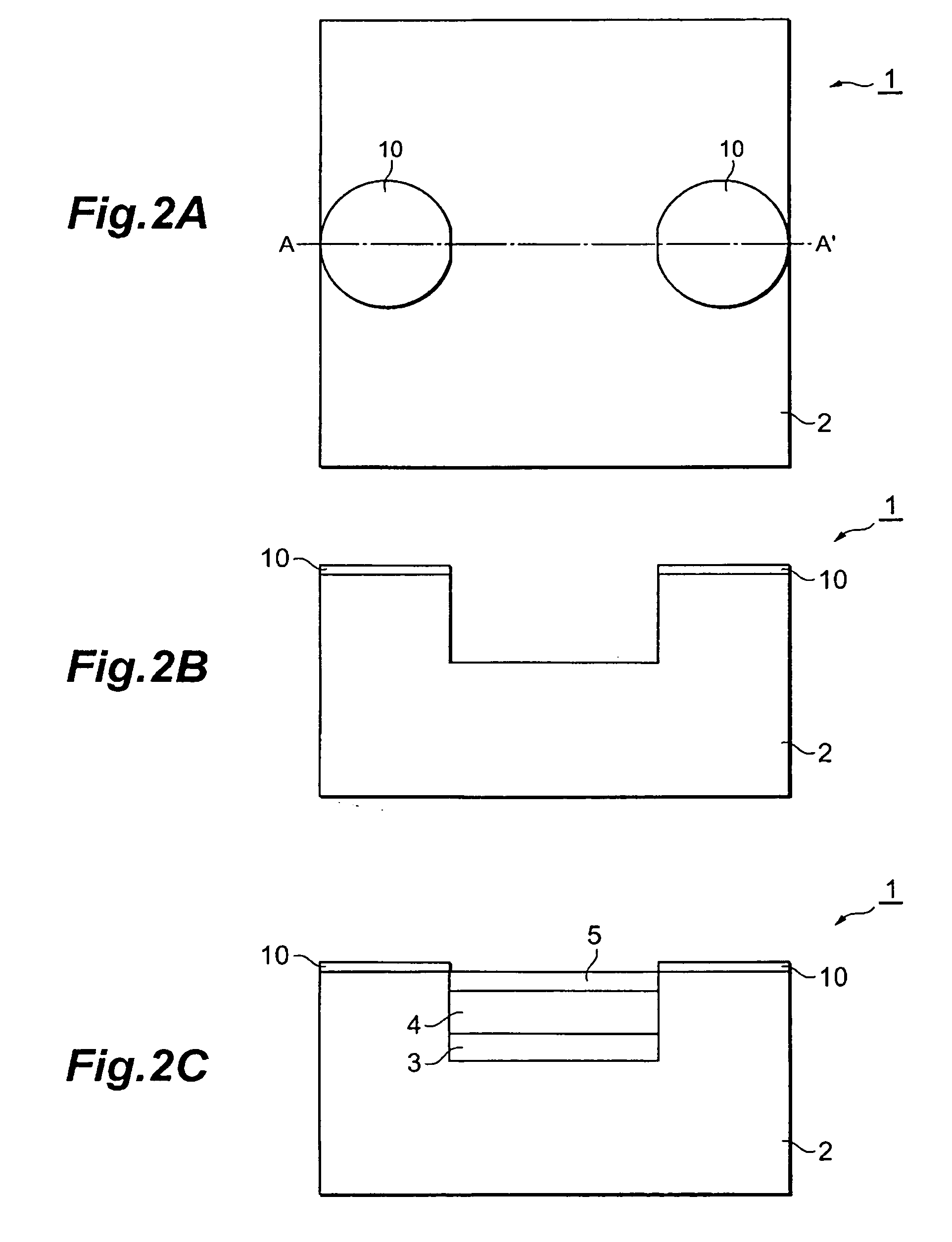
[0027]FIG. 1A is a schematic plan view of semiconductor photodetector 1 in the first embodiment and FIG. 1B a schematic sectional view along chain line AA′ in FIG. 1A. First, the configuration will be described. As shown in FIG. 1B, a semi-insulating GaAs substrate 2 has three top surface portions with different heights (which will be referred to as “upper step surface,”“middle step surface,” and “lower step surface” and which will be denoted by 2u, 2m, and 2d, respectively, in FIG. 1B). The heights of the respective step surfaces are set in decreasing order of height: the upper step surface, the middle step surface, and the lower step surface, and a level difference between the upper step surface and the middle step surface is preferably about 1-5 μm (specifically, 2.5 μm). A level difference between the middle step surface and the lower step surface is preferably about 0.1-2 μm (specifically, 0.5 μm). The step surfaces are formed so that the upper step surface and the middle step ...

second embodiment

[0043] The second embodiment of the present invention will be described with reference to FIGS. 3A, 3B, 3C, 3D, and 3E. FIGS. 3A, 3B, and 3C are schematic sectional views of semiconductor photodetector 1 in the second embodiment of the present invention, and the steps of FIG. 3A, FIG. 3B, and FIG. 3C are carried out in the aforementioned order of steps {circle over (1)}, {circle over (2)}, and {circle over (3)}. FIG. 3A shows a cross section along AA′ in FIG. 3D, and FIG. 3C a view showing a cross section along AA′ in FIG. 3E.

[0044] In the second embodiment detailed description will be given about the shape of the etching cross section in the recess forming step, which was not described in the first embodiment. Specifically, the second embodiment illustrates a case where the shape of the etching cross section is an inverted mesa shape. Here the inverted mesa shape is a state in which distances between two sides forming side walls in the etching sectional shape increase toward the b...

third embodiment

[0048] The third embodiment of the present invention will be described below with reference to FIGS. 4A, 4B, 4C, 4D, and 4E. FIGS. 4A, 4B, and 4C are schematic sectional views of semiconductor photodetector 1 in the third embodiment of the present invention, and the steps of FIGS. 4A, 4B, and 4C are successively carried out in the same manner as in FIGS. 3A, 3B, and 3C. FIG. 4A corresponds to a cross section along AA′ in FIG. 4D, and FIG. 4C to a cross section along AA′ in FIG. 4E.

[0049] The third embodiment is different from the second embodiment in that the ohmic electrodes 6, 7 are arranged at an angle of approximately 90° around the recess being the lower step portion (with the recess in between) and in that sectional shapes are different between the two electrode sides.

[0050] As shown in FIG. 4C, the recess of the semi-insulating GaAs substrate 2 is formed so that only the p-side ohmic electrode 6 is of the inverted mesa shape, out of the two side wall portions forming the se...


PUM


Abstract

In a semiconductor photodetector 1 according to the present invention, flat surfaces of three steps with different heights are formed in a top surface portion of a semi-insulating GaAs substrate 2. An n-type GaAs layer 3, an i-type GaAs layer 4, and a p-type GaAs layer 5 are successively deposited on the lower step surface formed in a central region of the semi-insulating GaAs substrate 2. Furthermore, a p-side ohmic electrode 6 is provided astride and above a flat surface formed by the p-type GaAs layer 5 and the upper step surface of the semi-insulating GaAs substrate 2, and an n-side ohmic electrode 7 is provided astride and above a flat surface formed by the n-type GaAs layer 3 and the middle step surface of the semi-insulating GaAs substrate 2.

Description

TECHNICAL FIELD [0001] The present invention relates to a semiconductor photodetector and a method of production thereof. BACKGROUND ART [0002] The conventional photoelectric conversion elements such as photodiodes (PDs) and avalanche photodiodes (APDs) are fabricated by forming pn-junction semiconductor layers on a high-density p-type or n-type semiconductor substrate by crystal growth, impurity diffusion, and so on. In recent years, in terms of high photosensitivity and high response, semiconductor photodetectors in which electrodes containing bonding pads for electrical connection with electrodes are provided on a semi-insulating substrate have been developed and are in practical use. [0003] For example, Japanese Patent Application Laid-Open No. 63-285971 (Document 1) discloses a semiconductor photodetector in which two types of semiconductor layers with different characteristics are exposed on an identical plane of a semi-insulating substrate to enable placement of electrodes on...

Claims


Application Information

Patent Timeline
Patent Type & Authority Applications(United States)
IPC IPC(8): H01L21/306H01L31/0224H01L31/0352H01L31/10H01L31/105
CPCH01L31/022416Y02E10/50H01L31/105H01L31/035281
Inventor NAKAJIMA, KAZUTOSHI
Owner HAMAMATSU PHOTONICS KK
Why Eureka
Try Eureka