Organic EL element array
- Summary
- Abstract
- Description
- Claims
- Application Information
AI Technical Summary
Benefits of technology
Problems solved by technology
Method used
Image

Examples
example 1
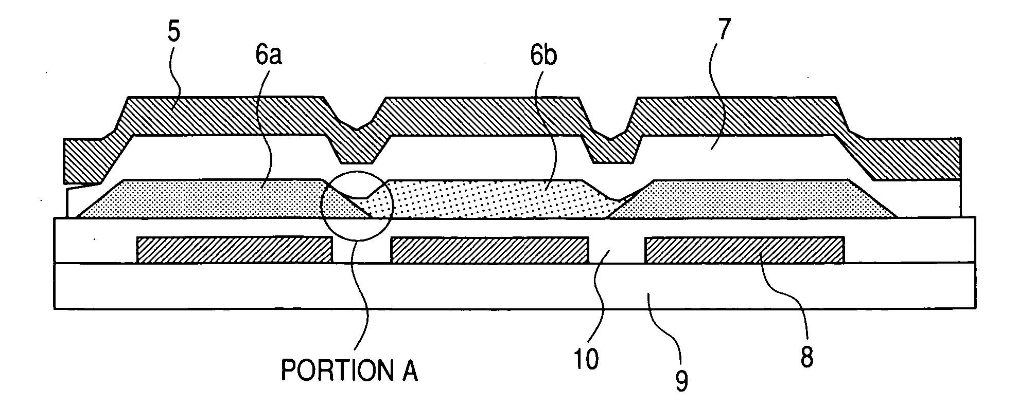
[0059] A multicolor light-emitting element of the structure shown in FIG. 2 was prepared. In this example, only light-emitting layers having emission spectrums of two colors of green and red were formed as the light-emitting layers 6a and 6b.
[0060] A glass substrate (Corning 1737 (trade name) manufactured by Corning Inc.) (transparent substrate 9) having an ITO layer of 100 nm in thickness formed thereon was prepared and patterned by means of photolithography to form the anode (transparent electrode 8) thereby forming an ITO substrate.
[0061] An organic compound layer and an electrode layer were continuously formed on the ITO substrate in a vacuum chamber of 10−4 Pa by means of vacuum evaporation using resistive heating to obtain an element A. A mask used for evaporation had a thickness of about 20 μm.
[0062] The materials used and film thicknesses for the respective layers are shown in Table 1 below. In this example, the hole-transporting layer corresponds to the first electron-tr...
example 2
[0072] A multi-color light-emitting element B was prepared by following substantially the same procedure as in Example 1 with the exception that the order of formation of the green-light-emitting layer and red-light-emitting layer in Example 1 was changed, that is, a mixture layer using CBP as a host and Ir(piq)3 as a guest was used as a first light-emitting layer and a mixture layer using Alq3 as a host and Coumarin 6 as a guest was used as a second light-emitting layer.
[0073]FIG. 6 shows the relation between an electrode width, an electrode interval, and film formed regions. FIG. 6 illustrates two electrodes of the same shape and first and second light-emitting layers disposed on the two electrodes respectively. In the figure, reference numeral 24 denotes a first light-emitting layer, 25 denotes a second light-emitting layer and 26 denotes pixel electrodes. That is, as illustrated in the figure, in this example, an electrode pitch was set to 45 μm, an electrode width was set to 2...
example 3
[0077] In this example, a multicolor light-emitting element was prepared which had a configuration shown in FIG. 8, that is, a configuration for taking out light on the cathode side (top emission structure).
[0078] A Cr film was formed on a glass substrate (Corning 1737 (trade name) manufactured by Corning Inc.) (transparent substrate 40) by sputtering in a thickness of 100 nm and patterned by a lift-off method to form an anode having light reflectivity (reflective electrode 39), thereby forming a substrate with a Cr electrode.
[0079] On this Cr substrate, organic compound layers (not illustrated) of the same constitution as described in Example 1 and a transparent electrode (cathode 35) were continuously formed in a vacuum chamber of 10−4 Pa through vacuum evaporation using resistive heating to obtain a multi-color light-emitting element C.
[0080] The thus formed element C did not cause any color mixing though showing a slight change in luminance at a periphery of the pixel electro...
PUM
 Abstract
Description
Claims
Application Information
 - Generate Ideas
- Intellectual Property
- Life Sciences
- Materials
- Tech Scout
- Unparalleled Data Quality
- Higher Quality Content
- 60% Fewer Hallucinations
Browse by: Latest US Patents, China's latest patents, Technical Efficacy Thesaurus, Application Domain, Technology Topic, Popular Technical Reports.
© 2025 PatSnap. All rights reserved.Legal|Privacy policy|Modern Slavery Act Transparency Statement|Sitemap|About US| Contact US: help@patsnap.com