Semiconductor storage device and production method therefor

a technology of semiconductor storage device and storage device, which is applied in the field of semiconductor storage device, can solve the problems of difficult enlargement of capacity, etc., and achieve the effect of enlargement of capacity, reducing writing current, and unsuitable enlargement of capacity

Inactive Publication Date: 2005-08-11
NEC CORP
View PDF11 Cites 41 Cited by
  • Summary
  • Abstract
  • Description
  • Claims
  • Application Information

AI Technical Summary

Benefits of technology

[0061] In a conventional method shown, for example, in FIGS. 17 to 21, a film (blanket film) forming a magnetic element such as a TMR is etched twice to remove a portion between the magnetic elements, further individual patterns of magnetic element cells are defined by an insulating process of the film forming the magnetic element, further lithography is required on a concave/convex surface, therefore miniaturization is difficult, and the method is unsuitable for enlargement of the capacity. On the other hand, according to the present invention, it is possible to define the pattern of the magnetic element by performing the lithog

Problems solved by technology

However, with the above-described conventional memory structure, it has been difficult to enlarge a capacity, a large writing current has been required, and it has been difficult to reduce power consumption.
In the lifting-off method, they can be approached, but miniaturization is difficult in this technique, and it is difficult to enlarge the capacity.
In the method of making the via

Method used


Image

  • Semiconductor storage device and production method therefor
  • Semiconductor storage device and production method therefor
  • Semiconductor storage device and production method therefor

Examples


first embodiment

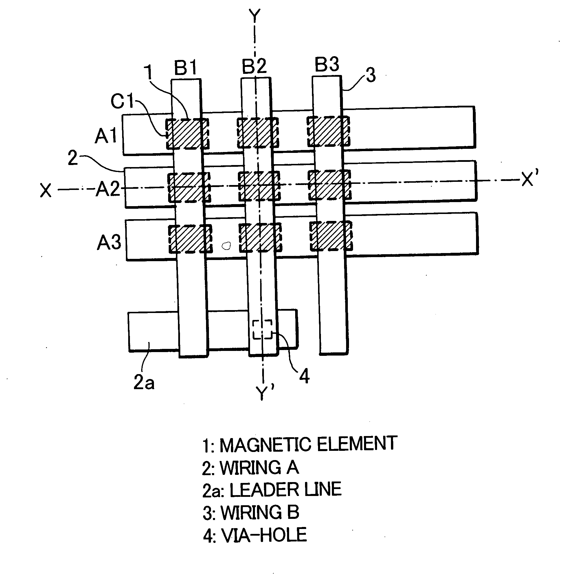
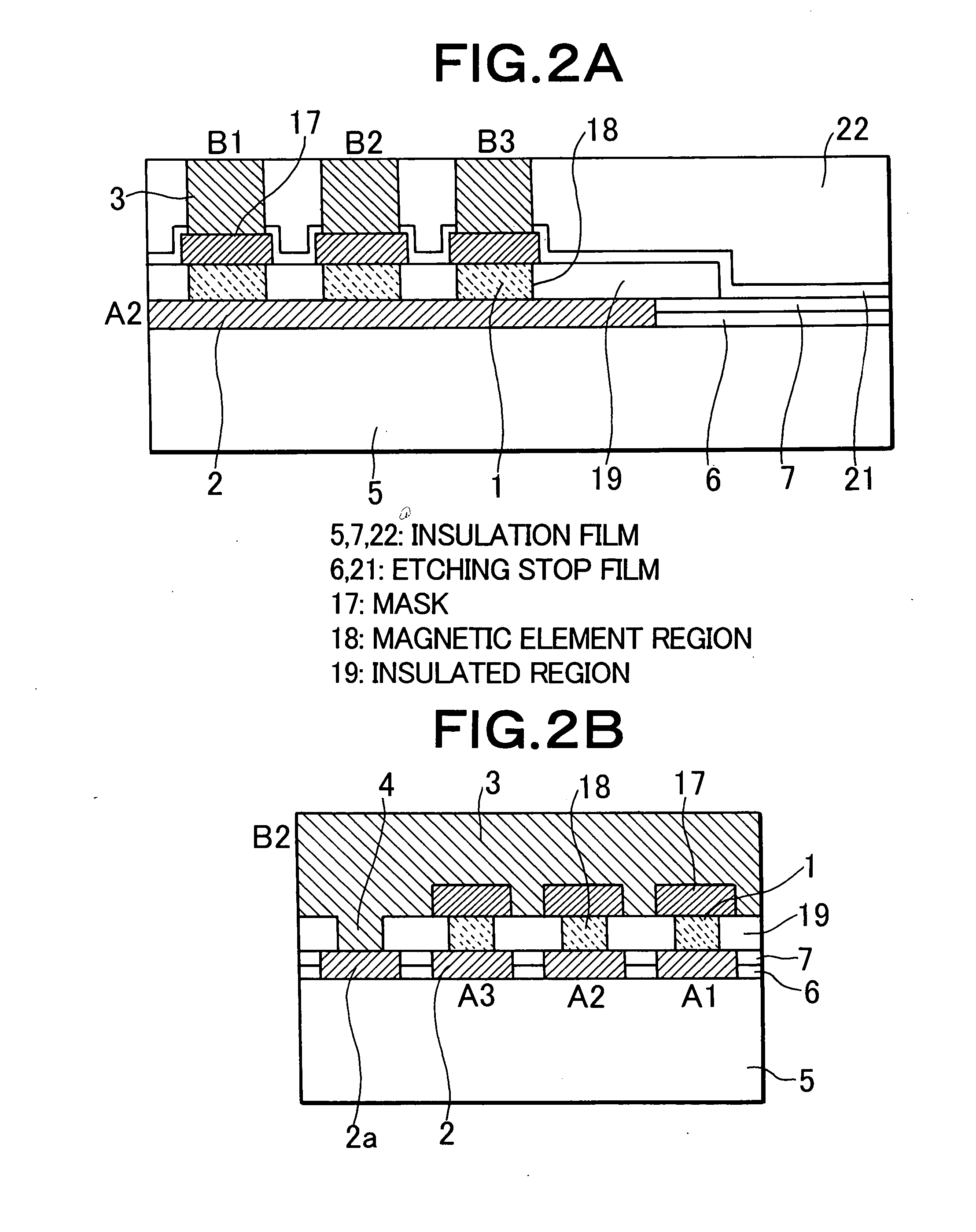
[0115]FIG. 1 shows a main part plan view of a semiconductor storage device according to a first embodiment of the present invention. As shown in FIG. 1, the semiconductor storage device has a plurality of magnetic elements 1, writing wiring A (A1 to A3):2 of two systems disposed in the vicinity of the respective magnetic elements, and wiring B (B1 to B3):3. Directions of the writing wirings A:2 of two systems and the wirings B:3 are different from each other. FIGS. 2A and 2B show sections of a wiring A direction (X-X′ line direction) and a wiring B direction (Y-Y′ line direction) of FIG. 1. Electric circuits are formed in a layer below (lower layer: not shown) and a layer above (upper layer: not shown) a constitution shown in FIGS. 2A and 2B, and the electric circuit is electrically connected to the magnetic elements described with reference to these figures to control operations of the magnetic elements. In the semiconductor storage device described in the embodiment of the present...

second embodiment

[0128]FIG. 5 shows a main part sectional view of a semiconductor storage device which is a second embodiment of the present invention. A plan view of the semiconductor storage device of the present embodiment is similar to that of FIG. 1 of the first embodiment, and FIG. 5 corresponds to a sectional view along line X-X′ of FIG. 1. As shown in FIG. 5, the semiconductor storage device of the present embodiment has a plurality of magnetic elements 1, and writing wiring A:2 (A2) and writing wiring B:3 (B1 to B3) of two systems disposed above / under each element. Laying directions of the writing wirings A, B of two systems are different from each other. Electric circuits are formed in a layer below (lower layer: not shown) and a layer above (upper layer: not shown) the constitution shown in FIG. 5, and the electric circuits are electrically connected to the shown magnetic elements to control operations of the magnetic elements.

[0129] In the semiconductor storage device of the present emb...

third embodiment

[0134]FIG. 7 shows a main part sectional view of a wiring structure of a semiconductor storage device which is a third embodiment of the present invention. A wiring of the semiconductor storage device has a first wiring (wiring film) 25 and a second wiring (wiring film) 26. Two wiring films partially or entirely contact each other, and wiring directions of the wiring films in a contacted portion substantially match each other (i.e., parallel wiring films are brought into close contact). This wiring structure is suitable for a wiring whose necessary portion is thickened. For example, when the structure is applied to the semiconductor storage device, all of the wiring for use in this device, or a portion on the magnetic element or in the vicinity of the magnetic element is thickened. In this case, when two wiring films are brought into close contact, one thick wiring is recognized. Therefore, when a current is passed in a wiring direction, a large amount of current flows in the vicini...


PUM


Abstract

Portions excluding magnetic elements of a laminate film of magnetic films or the like constituting magnetic elements (1) are oxidized/nitrided or oxynitrided to be insulated by a plasma processing using a conductive mask (17), whereby a plurality of magnetic elements are separated. This laminate film comprises a magnetic element region (18) formed with magnetic elements (1) and an insulated region (19) consisting of oxides/nitrides or oxynitrides. Upper wiring such as a bit line (3) is formed later. Since the conductive mask used in forming the insulated region is made part of the upper wiring, the magnetic elements and the upper wiring can be disposed in contact with each other.

Description

TECHNICAL FIELD [0001] The present invention relates to a semiconductor storage device (memory) in which an element (hereinafter referred to as a magnetic element) capable of changing a magnetized state, storing information by the magnetized state, and evaluating the magnetized state to thereby read stored information is used as a storage cell. BACKGROUND ART [0002] In this type of semiconductor storage device, for example, a magnetoresistive element has heretofore been used as a storage element. As an example of the magnetoresistive element, an element referred to as a tunneling magnetoresistance element (hereinafter referred to as TMR) will be described. In this element, a tunneling insulation film is held between two magnetic layers, and information is stored by resistance of the tunneling insulation film, which changes with a state of magnetization of the magnetic layers. [0003]FIG. 15 shows an example of the TMR reported in 2000 IEEE International Solid-State Circuits Conferenc...

Claims


Application Information

Patent Timeline
IPC IPC(8): H01F10/32H01F41/30H01L21/8246H01L27/22H01L43/08
CPCB82Y10/00B82Y25/00B82Y40/00H01L43/08H01F41/303H01L27/228H01F10/3254H10B61/22H10N50/10
Inventor KATOH, YUUKOH
Owner NEC CORP
Why Eureka
Try Eureka