

Composition for forming an electron emission source for use in an electron emission device and an electron emission source prepared therefrom
a technology of emission source and electron emission source, which is applied in the manufacture of electrode systems, electric discharge tubes/lamps, and screens, etc., can solve the problems of limited production of large-scale field emission devices, high cost, and high cost of carbon materials, and achieves superior electron emission efficiency, increased effective radiation area, and superior adhesive force
Inactive Publication Date: 2005-08-18
SAMSUNG SDI CO LTD
View PDF6 Cites 21 Cited by
- Summary
- Abstract
- Description
- Claims
- Application Information
AI Technical Summary
Benefits of technology
[0010] In one embodiment of the present invention, a composition is provided for forming an electron emission source for use in an electron emission device, the electron emission source having superior adhesive force and an increased effective radiation area, thereby offering superior electron emission efficiency.
Problems solved by technology
However, since the spindt-type electron emission source has an ultra-fine structure, the method of fabricating it is very complicated and requires a great deal of attention.
Therefore, it is limited in producing large-sized field emission devices.
However, carbon materials are generally very unstable at temperatures of 400° C. or higher and in the presence of oxygen, and a lot of carbon nanotube is lost during sintering.
This results in a reduced number of sites contributing to emission, which makes the carbon nanotube unsuitable for use as an electron emission source.
The result is reduced emission capability and life cycle of the electron emission device.
However, if the solid content is increased to increase the film thickness after sintering, the relative content of the carbon nanotube increases greatly, and the exposed part of the carbon nanotube paste becomes too thin.
Accordingly, it is difficult to increase the content of the carbon nanotube to obtain a high emission current density.
However, when an electron emission source is fabricated using the resultant carbon nanotube paste, the exposure thickness decreases and the amount of the carbon nanotube remaining after sintering decreases, so that it is difficult to obtain a carbon nanotube electron emission source having an ideal thickness.
However, if the thick film surface is covered by the fine metal powders, the field emission capability is not fully realized.
However, this method requires stabilization time to stabilize the photosensitive material against field emission.
Method used
View moreImage
Smart ImageViewing Examples

Examples
example 1
[0050] An electron emission source was prepared as in comparative Example 1, except 4 g vinyltrimethoxyethoxysilane was used in place of glass frit.
example 2
[0051] An electron emission source was prepared as in Comparative Example 1, except 4 g vinyltrimethylsilane was used in place of glass frit.
example 3
[0052] An electron emission source was prepared as in Comparative Example 1, except 4 g vinyltrimethoxysilane was used in place of glass frit.
Login to View More PUM
| Property | Measurement | Unit |
|---|---|---|
| Percent by mass | aaaaa | aaaaa |
| Percent by mass | aaaaa | aaaaa |
| Percent by mass | aaaaa | aaaaa |
Abstract
The present invention relates to a composition for forming an electron emission source for use in an electron emission device and an electron emission source prepared therefrom. The composition comprises an organic binder resin, a carbon-based material, a solvent and a silane-based compound. Also provided is a photosensitive composition for forming an electron emission source comprising an organic binder resin, a carbon-based material, a solvent, a photosensitive component selected from the group consisting of photosensitive monomers, photosensitive oligomers and photosensitive polymers, a photoinitiator and a silane-based compound of the general form R′—SiR3, where R is selected from the group consisting of alkoxys, alkyls, chloro, fluoro and bromo, and R′ is selected from the group consisting of vinyl, epoxy, methacryl, amino, mercapto and 2-(3,4-epoxycyclohexyl)ethyl. The composition imparts superior adhesive force, thereby increasing the effective radiation area, and improving the electron emission efficiency of the electron emission device.
Description
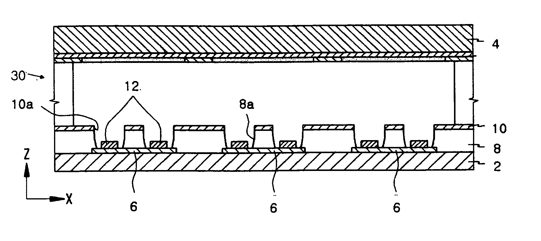
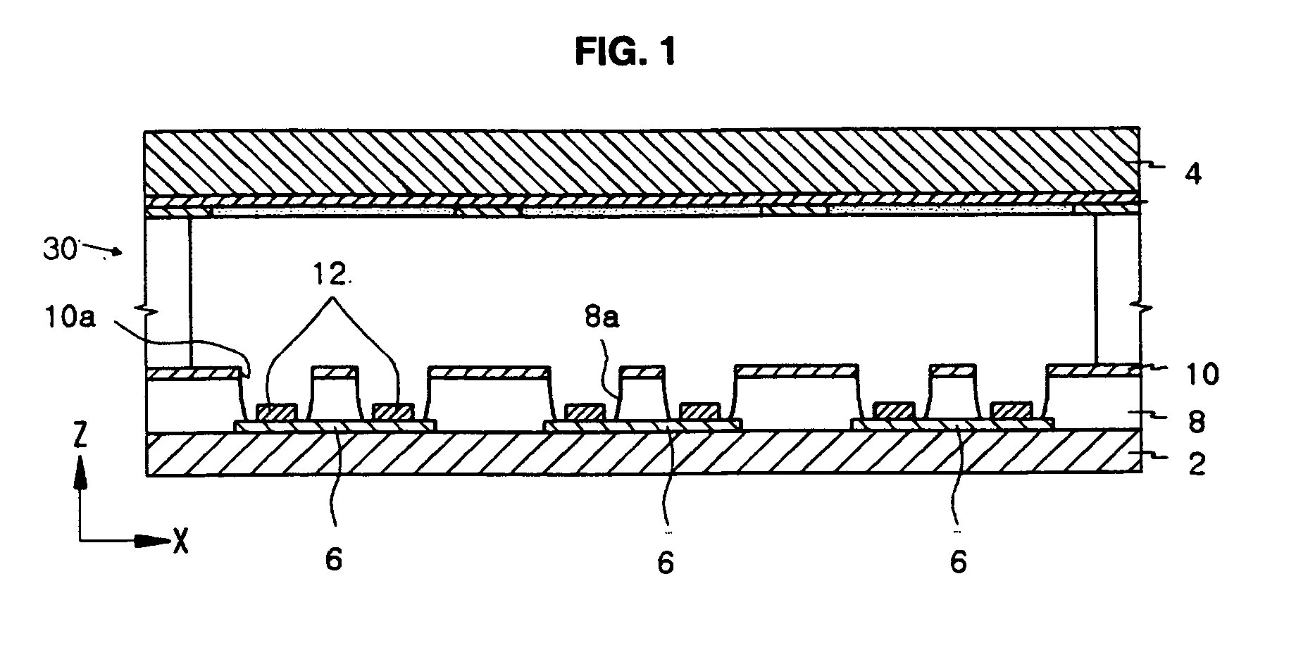
CROSS-REFERENCE TO RELATED APPLICATION [0001] This application claims priority of Korean Patent Application No. 10-2004-0001476, filed Jan. 9, 2004, the entire disclosure of which is incorporated herein by reference. FIELD OF THE INVENTION [0002] The present invention relates to a composition for forming an electron emission source for use in an electron emission device and an electron emission source prepared therefrom, and more particularly to a composition for forming an electron emission source for use in an electron emission device having good electron emission efficiency, superior adhesive force and improved effective radiation area, and an electron emission source prepared therefrom. BACKGROUND OF THE INVENTION [0003] Earlier electron emission sources for use in electron emission devices comprised spindt-type electron emission sources including one of molybdenum, silicon, etc., with sharp tips of sub-micron size. However, since the spindt-type electron emission source has an ...
Claims
Login to View More Application Information
Patent Timeline
 IPC IPC(8): H01J29/04C07F7/18C08K3/04C08K7/24C09K3/00H01J1/00H01J1/02H01J1/14H01J1/304H01J1/38H01J9/02H01J31/12
CPCB82Y10/00B82Y30/00C08K3/04H01J2201/30469C08K2201/011H01J1/304H01J2201/30446C08K7/24C08K3/041C08K3/045C08L33/12A01M13/003A01M2200/012
InventorYOO, SEUNG-JOONKIM, JAE-MYUNGNAM, JOONG-WOOLEE, SU-KYUNGMOON, JONG-WOONLEE, HYUN-JUNG
OwnerSAMSUNG SDI CO LTD