Optical connectors for electronic devices

a technology of optical connectors and electronic devices, applied in optics, instruments, optical light guides, etc., can solve the problems of limiting factors, overpowering data transfer apparatuses, and large digital signals, so as to avoid manufacturing costs typically associated with optical connectors, the output speed of the cable is no longer a limiting factor, and the effect of reducing the cost of optical connectors

Active Publication Date: 2005-08-18
II VI DELAWARE INC
View PDF51 Cites 84 Cited by
  • Summary
  • Abstract
  • Description
  • Claims
  • Application Information

AI Technical Summary

Benefits of technology

[0018] Since the manufacturer can substitute electrical wiring with optical wiring, the throughput speed of the cable is no longer a limiting factor when transferring large digital data from one component device to the next. In particular, the optical fiber avoids many of the disadvantages commonly known with metal wiring, such as limited throughput speed, resistance, impedance, EMI, and so forth. Furthermore, since the connector can be made without the use of a lens, a large part of the manufacturing costs typically associated with optical connectors can be avoided, making optical cables for use with conventional home electronic devices competitively priced.

Problems solved by technology

Nevertheless, although digital signals were initially smaller than conventional analog signals, present technology now uses digital signals that hold greater and greater amounts of information, such that digital signals are now becoming quite large.
This can overwhelm a data transfer apparatus that may be used to carry multiple digital video and audio signals at once.
Accordingly, conventional cabling between electronic devices is becoming a limiting factor, despite the ever-improving storage and playback capabilities of the connected electronic devices.
Unfortunately, DVI and HDMI cables also tend to be very expensive, are based on metal wiring, and are rather large and bulky, particularly if used for distances of more than a few feet.
This can become a complication if a home user desires to wire one HD component in one room of a home to another room of a home.
In particular, DVI and HDMI cables cannot be easily routed in a home at least in part since they have a stringent bend radius, and have other similar requirements that can complicate installation.
Furthermore, the metallic composition of conventional DVI, HDMI, or even USB cables makes the cables susceptible to resistance, signal interference, and signal degradation, particularly over longer distances.
As a result, despite the improved capabilities of present digital storage or playback devices, even DVI, HDMI, and USB connectors could limit the extent to which large digital data can be effectively transferred, and thus used.
Unfortunately, these types of systems still present various problems and shortcomings that may render them less than ideal for high throughput digital transfers.
For example, infrared wireless networks depend on line-of-sight devices, and thus are not well suited for connecting devices that are located in different rooms, without strategic positioning of certain access points.
In addition, HomeRF systems are characterized typically by relatively slow data rates, (about 1 mbps), have fairly limited range (about 75 to 125 feet), and can be difficult to integrate together within existing wired networks.
Unfortunately, the difficulty associated with precisely aligning optical fibers, and the lenses used within a relevant transmitter or receiver optical assembly, make conventional optical fibers less suitable for present consumer electronic applications.
In particular, the manufacturing costs of aligning conventional optical components, such as an optical lens, at the appropriate fault tolerances between an optical fiber and a transmitter or receiver component would render conventional optical cables far too expensive for most consumer use.

Method used


Image

  • Optical connectors for electronic devices
  • Optical connectors for electronic devices
  • Optical connectors for electronic devices

Examples


Embodiment Construction

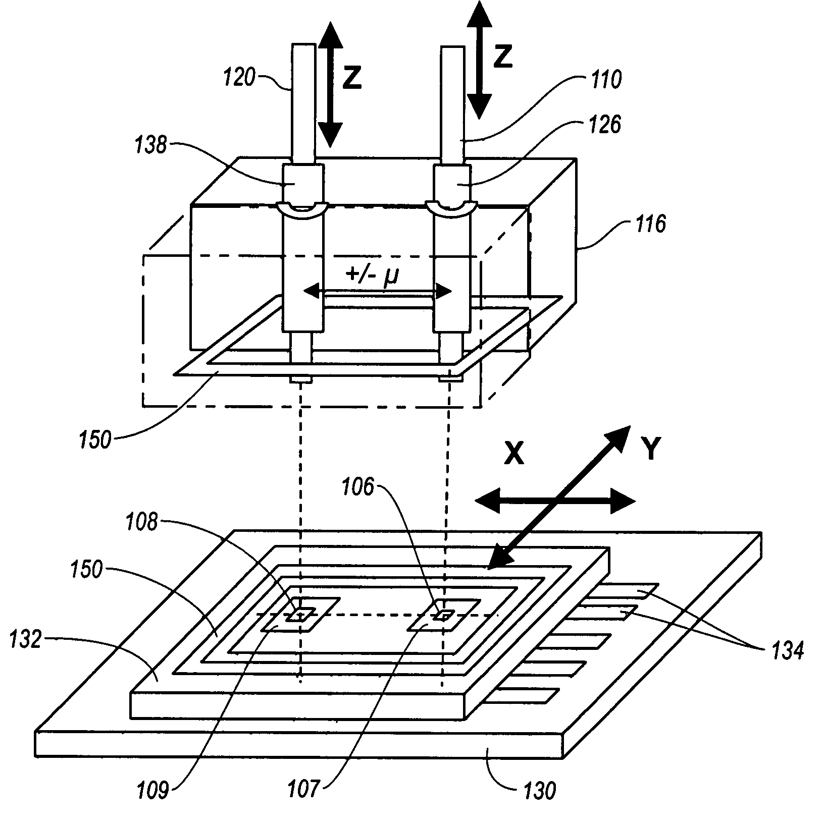
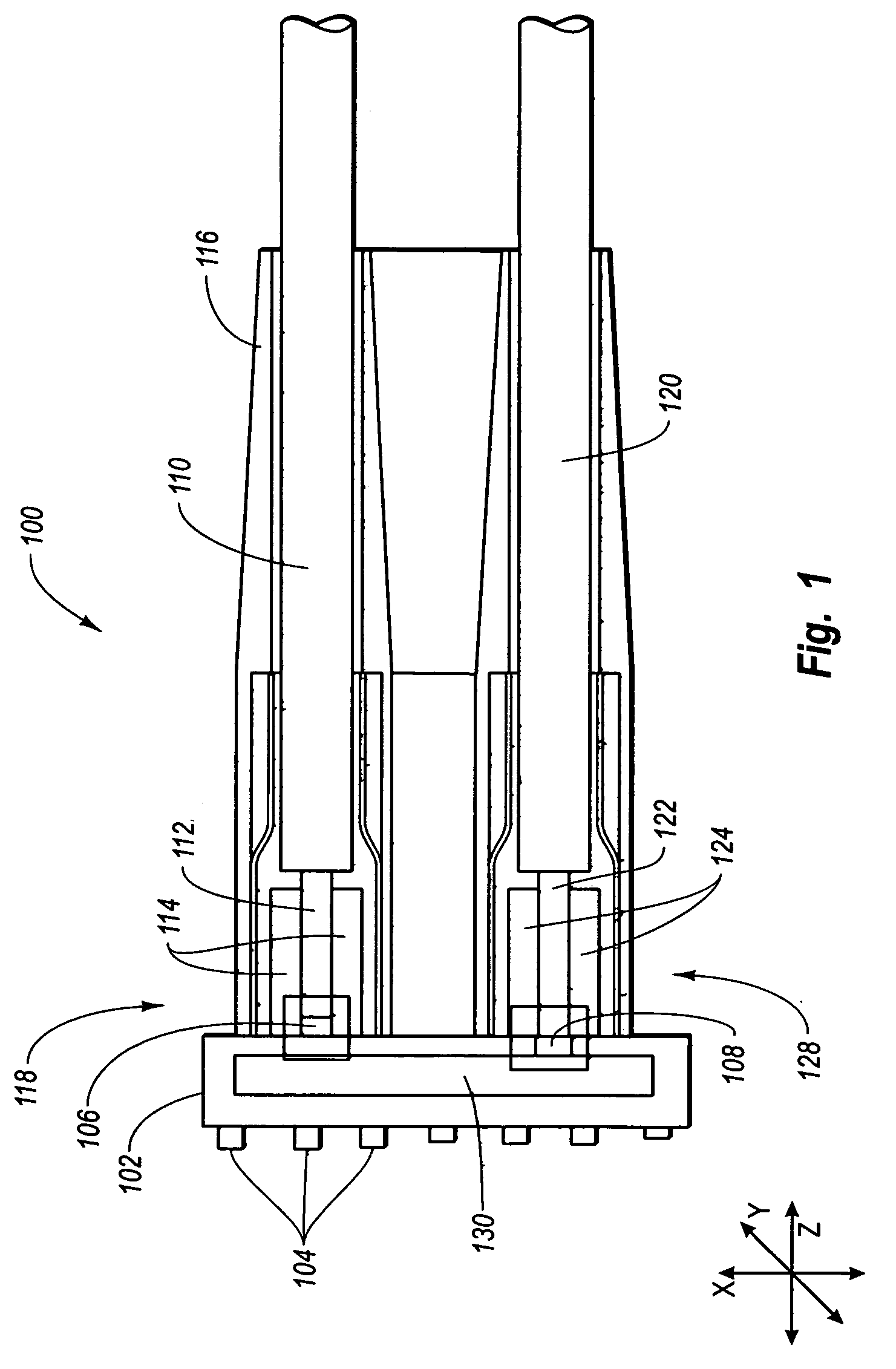
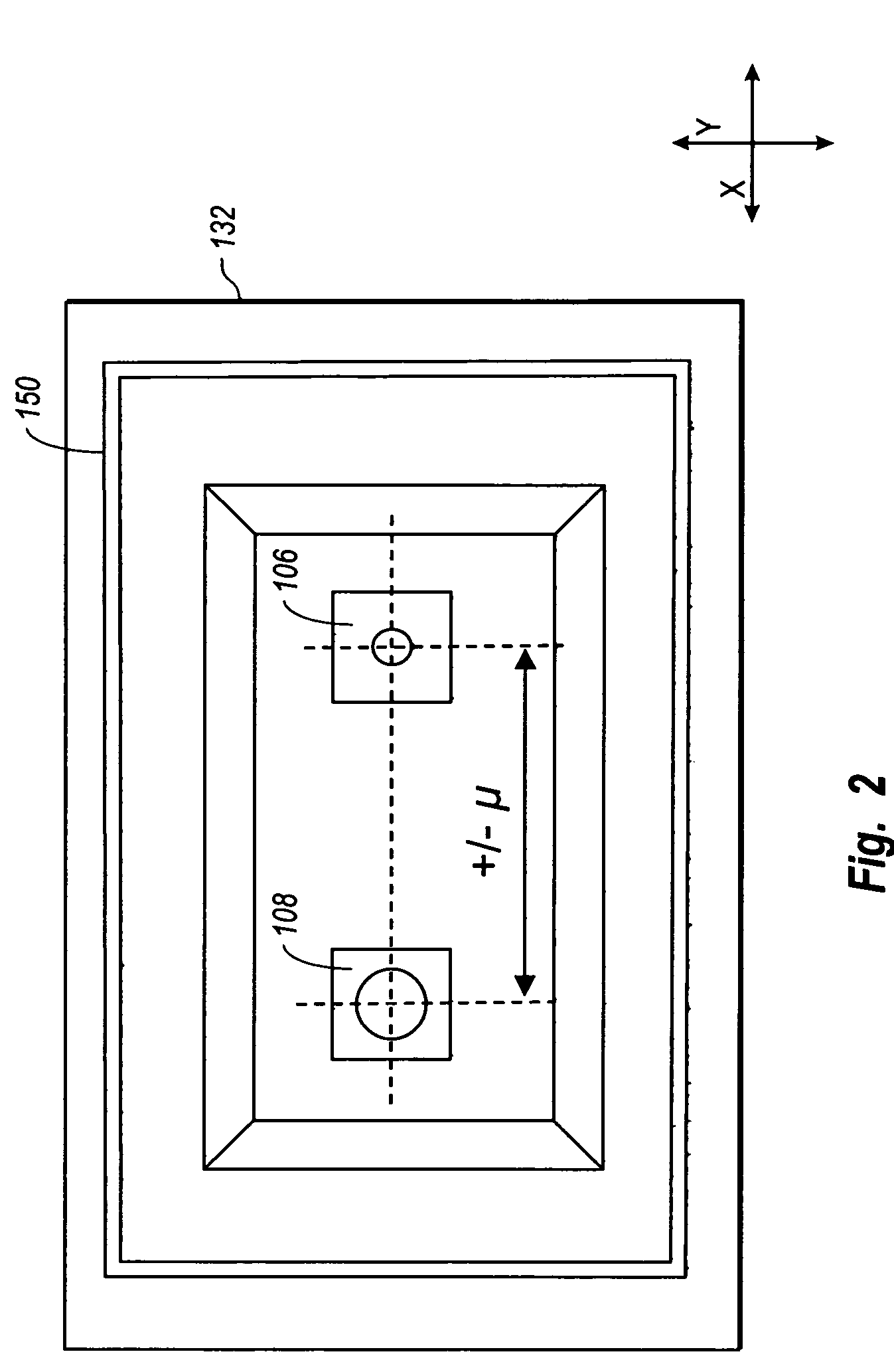
[0015] The present invention addresses one or more of the foregoing, and other, problems in the art by replacing much of the metallic wiring in conventional digital data transfer connectors with optical fiber. In particular, exemplary embodiments of the present invention include optical cables having an optical transceiver embedded within the electrical connection interface, such as a USB, HDMI, or DVI without using a lens between the optical fiber and optical transceiver components.

[0016] For example, in accordance with one implementation of the present invention, an electrical connector interface, such as a USB, HDMI, or DVI connection interface includes a built-in optical transceiver having a Transmit Optical Sub-Assembly (“TOSA”) positioned therein. The TOSA includes a Vertical Cavity Surface Emitting Laser (“VCSEL”), and a multi-mode optical fiber positioned relatively close to the VCSEL. The VCSEL is positioned to have a numerical aperture less than that of the corresponding ...


PUM


Abstract

A high-data rate connector for use with consumer electronics couples digital electrical connection interfaces with optical cabling and optical transceivers. In one implementation, an electrical connection interface, such as a DVI, HDMI, or USB connection interface is electrically coupled to an optical transceiver. The optical transceiver includes an optical transmitter, such as a VCSEL, and an optical detector, such as a photodiode. The transmit fiber and the receive fiber are each positioned relatively close to the corresponding optical transmitter and optical detector without a lens. The optical transmitter and the optical detector are each optimized for the size of the optical fiber core to enable high throughput speed at relatively low cost.

Description

CROSS REFERENCE TO RELATED APPLICATIONS [0001] This application claims the benefit of U.S. Provisional Patent Application No. 60 / 529129, filed Dec. 12, 2003, entitled “Systems and Devices for an Optical Home Network”, and U.S. Provisional Patent Application No. 60 / ______ (Workman Nydegger Attorney Docket No. 15436.282.1), filed on Dec. 8, 2004, entitled “Optical Connectors and Cables for Home Electronics”. All of the aforementioned applications are incorporated herein in their respective entireties by this reference.BACKGROUND OF THE INVENTION [0002] 1. The Field of the Invention [0003] The present invention relates generally to digital connectors, such as may be used between audio or video components of a home entertainment system, as well as between components in a personal computing system. [0004] 2. Background and Relevant Art [0005] Present consumer electronics are designed to store, process, and playback increasingly larger amounts of data. One reason for this is a present tre...

Claims


Application Information

Patent Timeline
Patent Type & Authority Applications(United States)
IPC IPC(8): G02B6/36G02B6/42
CPCG02B6/4224G02B6/4246G02B6/4239
Inventor FARR, MINA
Owner II VI DELAWARE INC
Why Eureka
Try Eureka