Stamper original and its manufacturing method, stamper and its manufacturing method, and optical disk
- Summary
- Abstract
- Description
- Claims
- Application Information
AI Technical Summary
Benefits of technology
Problems solved by technology
Method used
Image
Examples
example 1
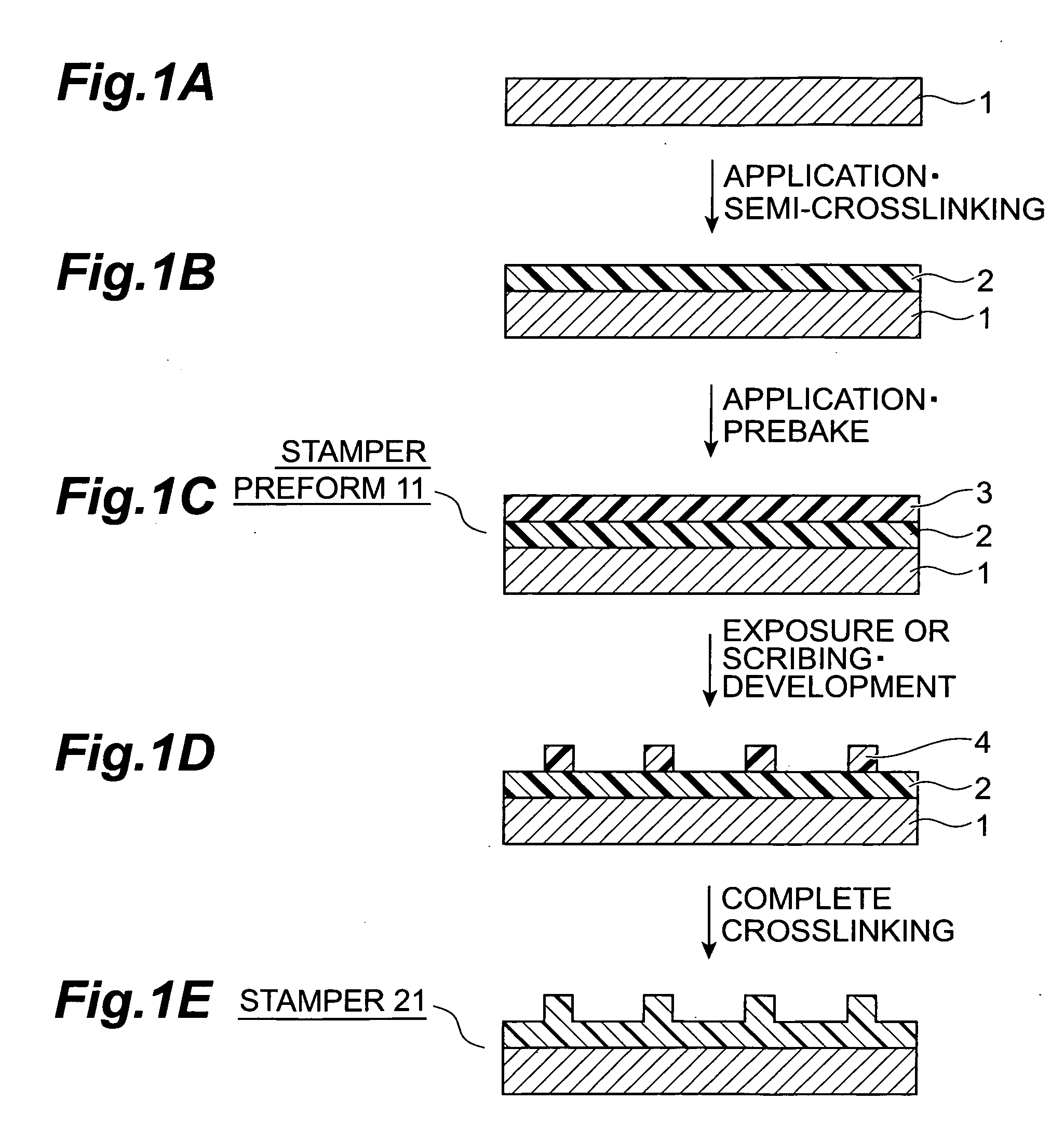
[0084] First, one surface of an Ni base with the outside diameter of 200 mm and the thickness of 0.3 mm was mechanically polished using cerium oxide (CeO2). Then an alkali-soluble negative resist containing a compound represented by Formula (1) below (NNR600S2, available from Nagase ChemteX Corporation) was applied in the thickness of 200 nm onto the polished surface of the Ni base by a spin coater.
[0085] After the application, the resist was treated in a hot plate set at 110° C., for two minutes to be thermally crosslinked, and, after / before the heating, the resist was exposed to UV light to be optically crosslinked, thereby forming a semi-crosslinked resist layer. Then an alkali-soluble negative resist containing a methoxymethyl melamine resin represented by foregoing Formula (1) (NNR600S2, available from Nagase ChemteX Corporation) was applied in the thickness of 200 nm onto the top surface of the semi-crosslinked resist layer by a spin coater and thereafter it was prebaked in ...
example 2
[0086] The prebaked resist layer of the stamper preform obtained was irradiated in a predetermined pattern with an Ar laser (351 nm) to record given information, and thereafter it was baked in a hot plate set at 110° C., for four minutes. Then a spin development was carried out at ordinary temperature (about 24° C.) for sixty seconds with a 1.57wt % TMAH aqueous solution to remove exposed portions, thereby forming resist bumps. Then the stamper preform with the resist bumps formed therein was subjected to multi-stage baking consisting of a treatment in a hot plate at 175° C. for ten minutes and a subsequent treatment in a hot plate at 250° C. for ten minutes. Furthermore, deep UV light was used to completely crosslink the semi-crosslinked resist layer and the resist bumps. Then the stamper preform was punched into a doughnut shape having the outside diameter of 138 mm and the inside diameter of 22 mm, thus producing a stamper.
example 3
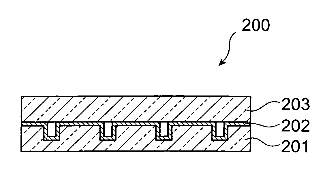
[0087] A polycarbonate resin was used as a material for the optical disk base. The stamper obtained in Example 2 above was mounted on a mold, and the injection compression molding was carried out to obtain an optical disk base in the outside diameter of 120 mm and the inside diameter of 15 mm in which the information pattern recorded in the stamper was transcribed. Then aluminum sputtering was effected on the information pattern transcribed surface in the optical disk base to form a reflective film. Furthermore, a polycarbonate dummy base in the same size as the optical disk base was bonded onto the reflective film with an adhesive, thus producing an optical disk.
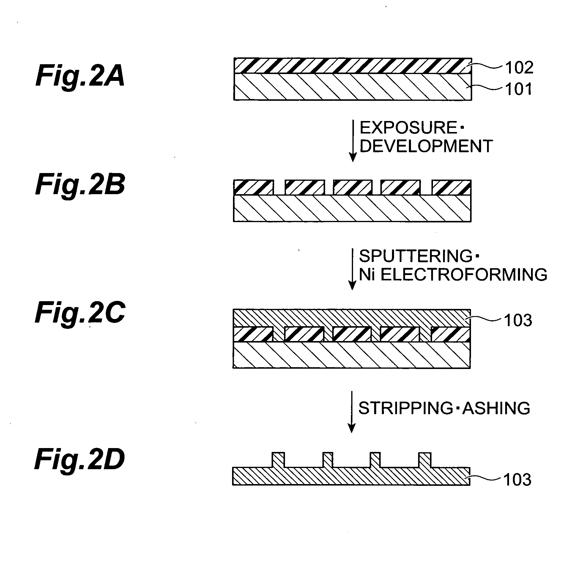
[0088] As described above, the stamper preform and the production method thereof, the stamper and the production method thereof, and the optical disk with the pattern transcribed by the stamper according to the present invention obviate the need for the Ni electroforming step taking the long time and readily producing a de...
PUM
| Property | Measurement | Unit |
|---|---|---|
| Electric charge | aaaaa | aaaaa |
| Wavelength | aaaaa | aaaaa |
| Exposure limit | aaaaa | aaaaa |
Abstract
Description
Claims
Application Information


