Manufacture of semiconductor device having nitridized insulating film

a technology of insulating film and semiconductor, which is applied in the direction of semiconductor devices, electrical devices, transistors, etc., can solve the problems of increasing gate leak current, increasing oxide film thickness, and difficult to control the amount of nitrogen concentration in each wafer and in the wafer

Inactive Publication Date: 2005-08-18
FUJITSU SEMICON LTD
View PDF9 Cites 12 Cited by
  • Summary
  • Abstract
  • Description
  • Claims
  • Application Information

AI Technical Summary

Benefits of technology

[0013] An object of the present invention is to provide a method of manufacturing a semicond

Problems solved by technology

As a gate insulating film becomes thin, tunneling current flows between the gate electrode and channel region, increasing gate leak current.
It can be considered that annealing in an N2O atmosphere may dissolve a porti

Method used


Image

  • Manufacture of semiconductor device having nitridized insulating film
  • Manufacture of semiconductor device having nitridized insulating film
  • Manufacture of semiconductor device having nitridized insulating film

Examples


Embodiment Construction

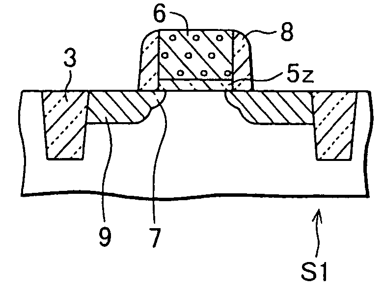
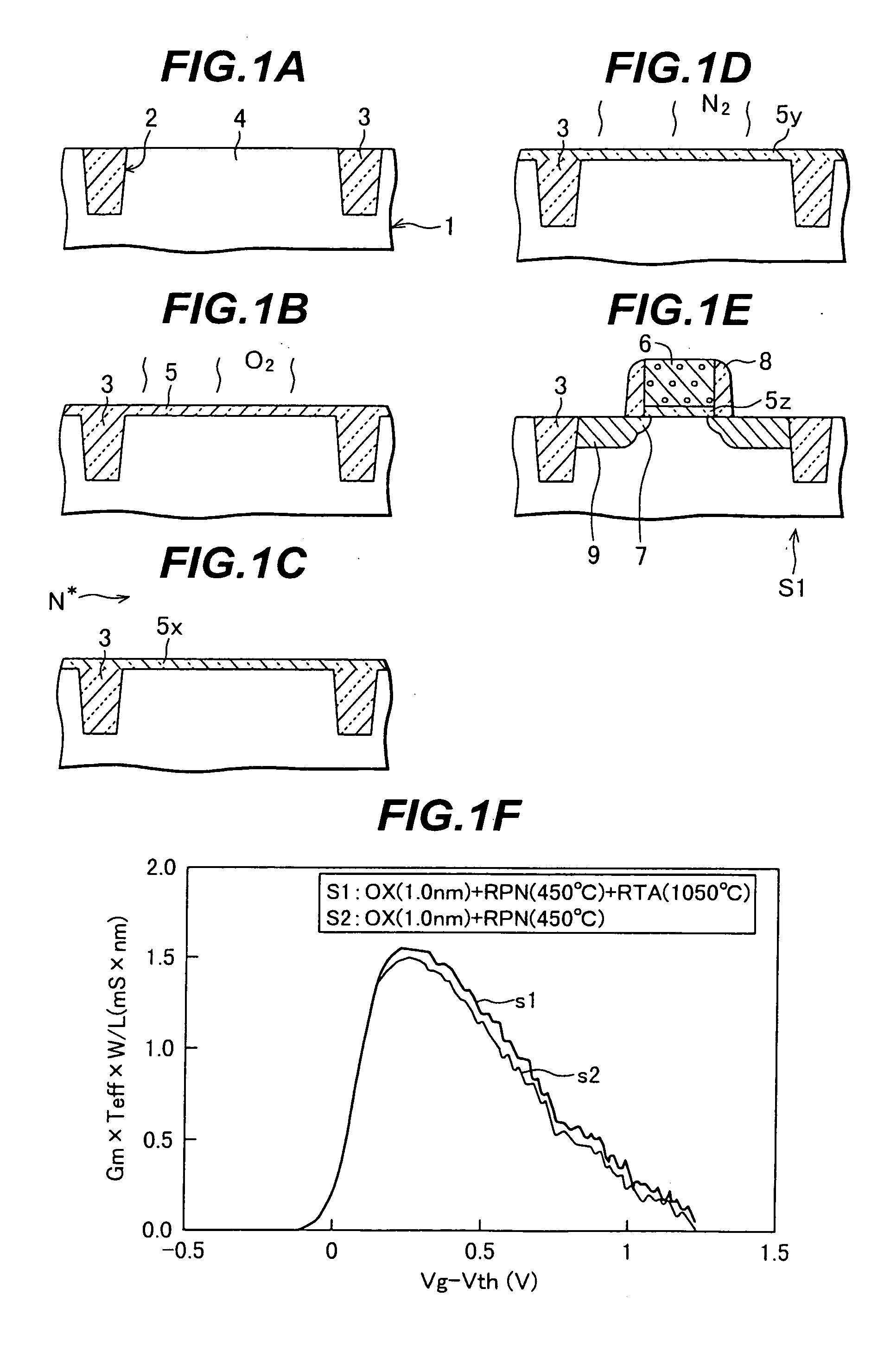
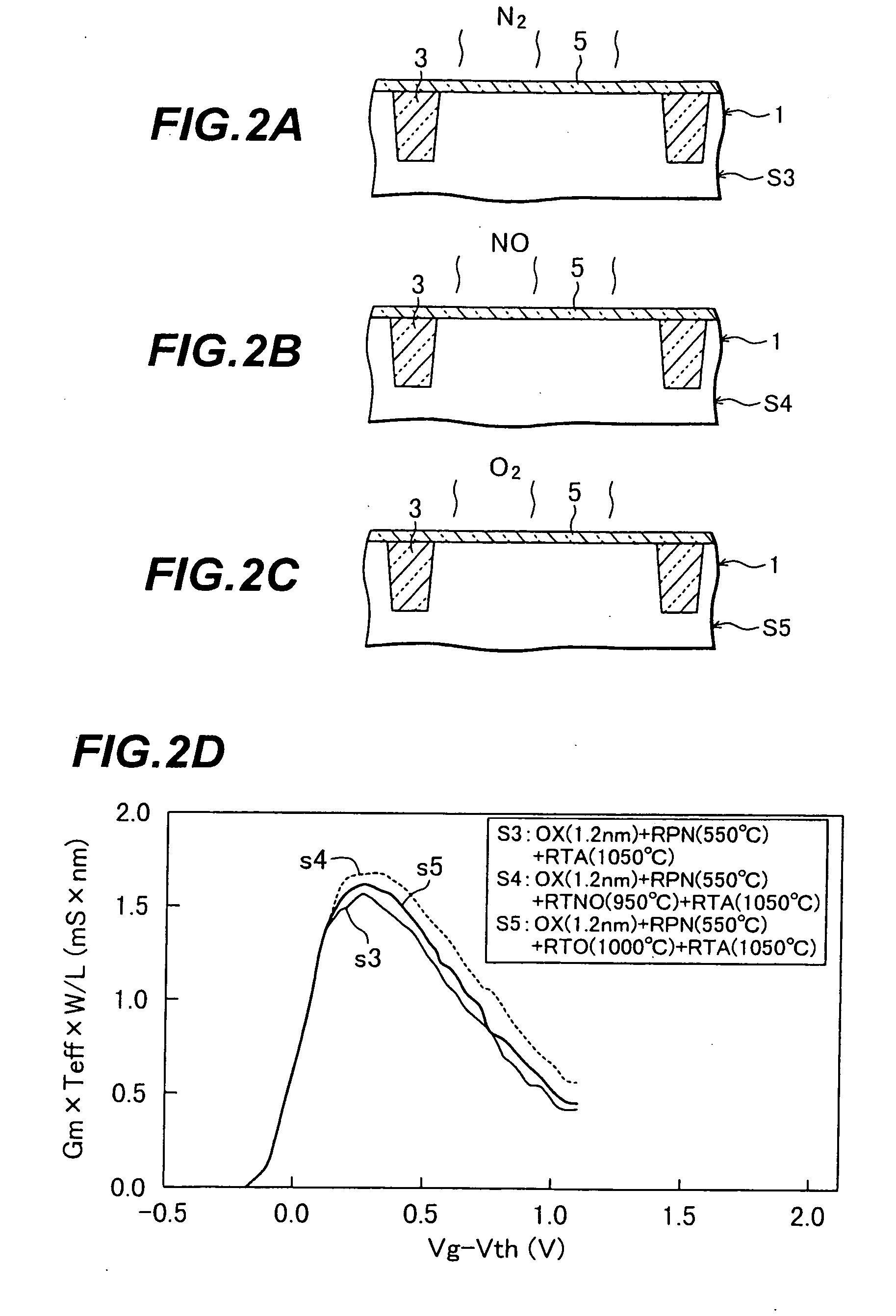
[0023] Nitrogen introduced into a gate insulating film of silicon oxide is effective for preventing boron from piercing through the gate insulating film during boron ion implantation into a gate electrode.

[0024] However, as the gate insulating film becomes thin, it is difficult to present boron ion piercing, and boron reaches the interface between the gate insulating film and silicon substrate. As boron enters the channel region, the mobility is lowered and the boron concentration at the interface is likely to become irregular.

[0025] By introducing active nitrogen generated by plasma into a silicon oxide film or silicon oxynitride film, a nitrogen concentration distribution can be obtained which has a peak on the insulating film surface or in the insulating film. By utilizing this plasma nitridizing, more nitrogen can be introduced while the nitrogen concentration at the interface with the substrate is suppressed. A high nitrogen concentration is effective for suppressing boron pi...


PUM


Abstract

A method for manufacturing a semiconductor device is disclosed which enables to suppress decrease in the mobility in a channel region by suppressing piercing of boron through a gate insulation film which boron is ion-implanted into a gate electrode. The method for manufacturing a semiconductor device includes: a step for forming a gate insulating layer on an active region of a semiconductor substrate; a step for introducing nitrogen through the front surface of the gate insulating layer using active nitrogen; and a step for conducting an annealing treatment in an NO gas atmosphere so that the nitrogen concentration distribution in the nitrogen-introduced gate insulating layer is high on the front surface side and low on the side of the interface with the semiconductor substrate.

Description

CROSS REFERENCE TO RELATED APPLICATION [0001] This application is a continuation application of PCT / JP2004 / 006213 filed on Apr. 28, 2004, which claims priority of PCT / JP03 / 05561 filed on Apr. 30, 2003, the entire contents of both of which are incorporated herein by reference.BACKGROUND OF THE INVENTION [0002] A) Field of the Invention [0003] The present invention relates to a semiconductor device manufacture method, and more particularly a method for manufacturing a semiconductor device having a gate insulating film which contains nitrogen. [0004] B) Description of the Related Art [0005] In order to improve the integration degree and operation speed of a semiconductor integrated circuit device, MOSFETs as its constituent elements are made micro fine and gate insulating films are made thinner. A gate electrode on the gate insulating film is usually made of a polysilicon layer or a lamination of a polysilicon layer and a silicide layer. Impurity ions are usually implanted into the pol...

Claims


Application Information

Patent Timeline
IPC IPC(8): H01L21/28H01L21/314H01L21/336H01L21/8238H01L29/51
CPCH01L21/28185H01L21/28202H01L21/3144H01L29/6659H01L21/823857H01L29/518H01L21/823842H01L21/0214H01L21/02318H01L21/0234H01L21/02329
Inventor HORI, MITSUAKI
Owner FUJITSU SEMICON LTD
Why Eureka
Try Eureka