
Light-emitting semiconductor device and method of fabrication

Inactive Publication Date: 2005-08-25
SANKEN ELECTRIC CO LTD
View PDF2 Cites 67 Cited by
  • Summary
  • Abstract
  • Description
  • Claims
  • Application Information

AI Technical Summary

Benefits of technology

[0011] The present invention has it as an object to improve the efficiency of light-emitting semiconductor devices, without the difficulties encountered heretofore.
[0014] The antidiffusion layer of any such composition has proved effective to bar the diffusion of the constituent element or elements of each of the ohmic contact layer and reflective layer into the other and hence to inhibit the creation of a region of alloys between these layers. Held against the ohmic contact layer via this antidiffusion layer, the reflective layer is therefore much more reflective than in the prior art case where it is held directly against the ohmic contact layer. The better reflection of the light by the reflective layer leads to a greater amount of light issuing from the device.

Problems solved by technology

One of the problems encountered with this conventional light-emitting device is that the GaAs substrate is highly absorptive of the light of the wavelength range emitted by the active semiconductor layers or the main semiconductor region of the light-emitting device.
This remedy proved unsatisfactory, however, as the active semiconductor layers and the transparent support substrate gave rise to electrical resistance at the interface therebetween.
This resistance made the forward voltage between the anode and cathode of the light emitting device inconveniently high.
However, this second recited prior art device also proved to have its own weaknesses.
One of these weaknesses arose in conjunction with the manufacturing process of the device, which involved several heat treatments.
Undesired reactions took place as a result of such heat treatments between the reflective metal layer and Au—Ge—Ga regions and the neighboring parts of the active semiconductor layers.
The result was a diminution of reflectivity at their interfaces.
High-efficiency light-emitting devices were therefore not obtainable with as high a yield as had been expected.
This construction is objectionable because it leads to a drop in reflectivity as the metal layer and the electrode are easy to make an alloying reaction through the open insulating layer.
Offsetting this advantage, however, is the difficulty of creating the current blocking region, which requires additional steps for LED production, adding substantively to its manufacturing cost.

Method used


Image

  • Light-emitting semiconductor device and method of fabrication
  • Light-emitting semiconductor device and method of fabrication
  • Light-emitting semiconductor device and method of fabrication

Examples


embodiment

of FIG. 3

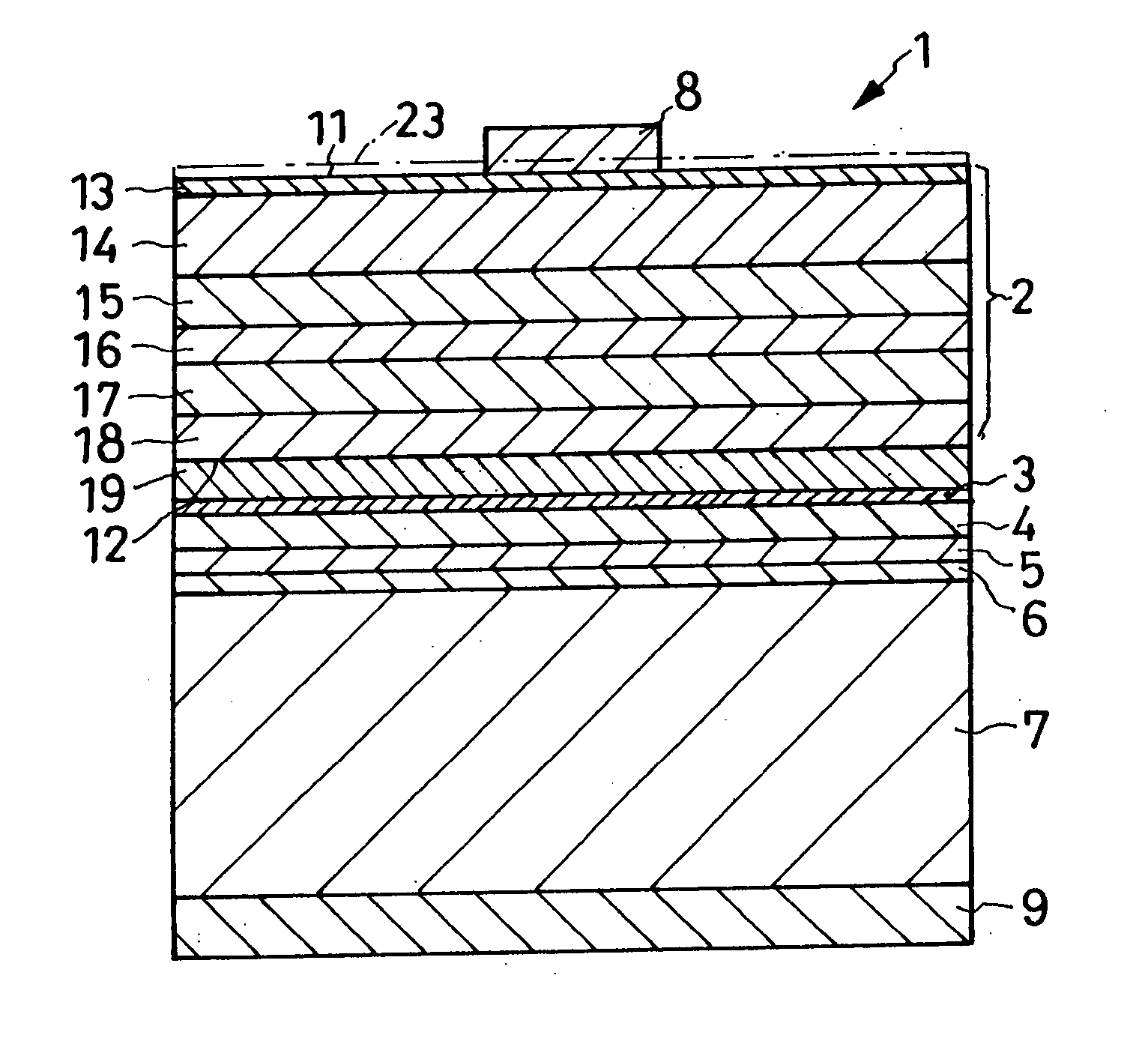
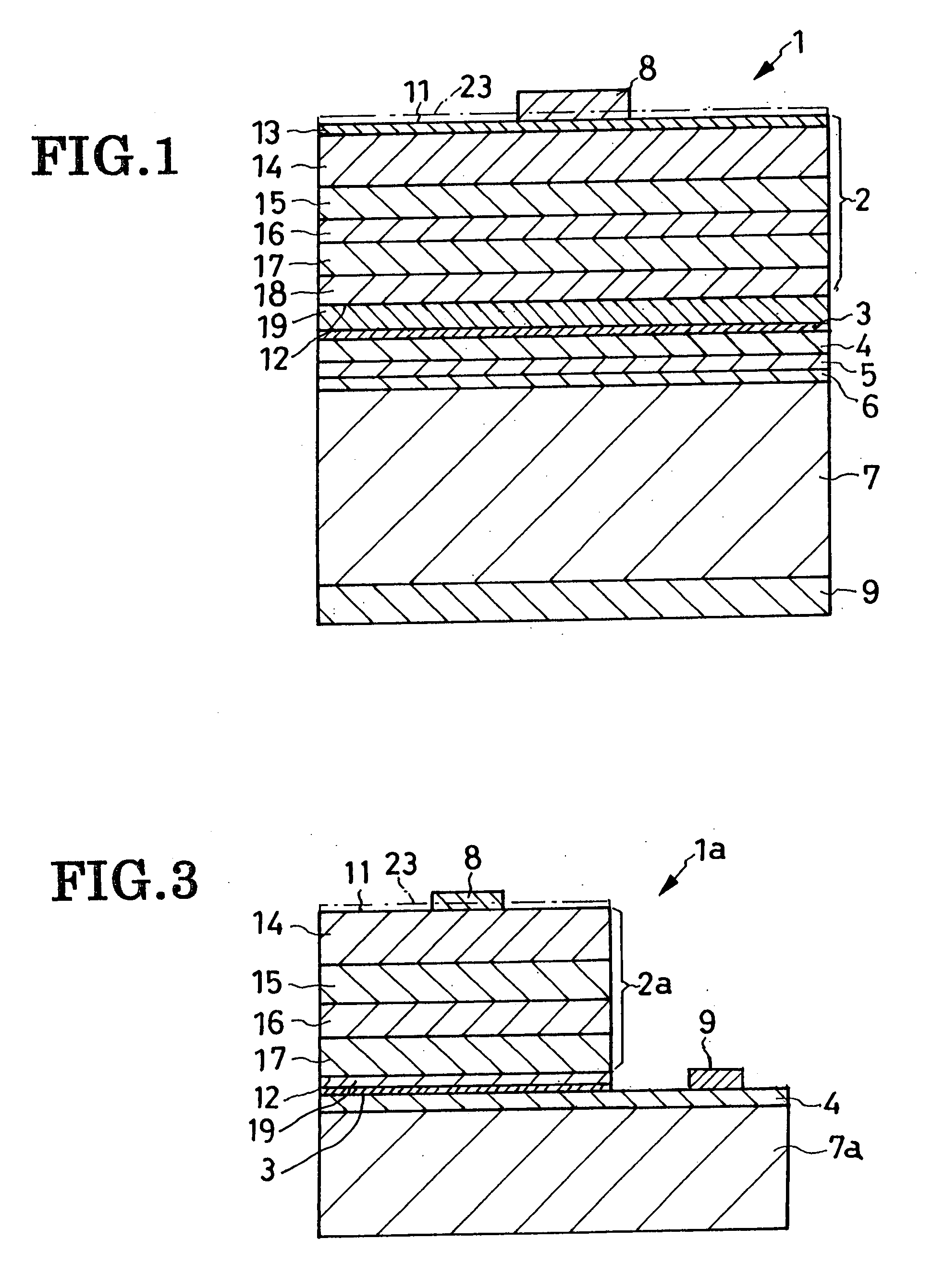
[0071]FIG. 3 illustrates another preferred form of LED 1a according to the invention, which differs from its FIG. 1 counterpart in having a modified semiconductor region 2a, modified baseplate 7a, and modified positioning of the anode 9. The modified semiconductor region 2a is akin to its FIG. 1 equivalent 2 except for the absence of the first and third complementary layers 13 and 18. The cathode 8 is therefore mounted on the surface 11 of the n-type complementary layer 14, which might be more aptly termed the current spreading layer in this alternate embodiment of the invention. Further, as the third complementary layer 18 is absent, the ohmic contact layer 19 makes ohmic contact with the p-type semiconductor region 17.

[0072] It will be further observed from FIG. 3 that the modified baseplate 7a and the reflective layer 4 thereon have portions projecting laterally beyond the overlying semiconductor region 2a. The anode 9 is placed on the ledge thus formed by the baseplate...


PUM


Abstract

An LED includes a semiconductor region having an active layer sandwiched between two confining layers of opposite conductivity types for generating heat. A cathode is arranged centrally on one of the opposite major surfaces of the semiconductor region from which is emitted the light. Attached to the other major surface of the semiconductor region, via an ohmic contact layer, is a reflective metal layer for reflecting the light that has traversed the ohmic contact layer, back toward the semiconductor region. A transparent antidiffusion layer is interposed between the ohmic contact layer and the reflective layer in order to prevent the ohmic contact layer and the reflective layer from thermally diffusing from one into the other to the impairment of the reflectivity of the reflective layer.

Description

CROSS REFERNCE TO RELATED APPLICATIONS [0001] This application claims priority to Japanese Patent Application No. 2004-050378, filed Feb. 25, 2004, and Japanese Patent Application No. 2004-264342, filed Sep. 10, 2004. BACKGROUND OF THE INVENTION [0002] This invention relates to a light-emitting semiconductor device, or light-emitting diode (LED) according to more common parlance, and more particularly to such devices having active layers made from chemical compounds such for example as aluminum gallium arsenide (AlGaAs), aluminum gallium indium phosphide (AlGaInP), gallium nitride (GaN), aluminum gallium indium nitride (AlGaInN), and derivatives thereof. The invention also concerns a method of making such light-emitting semiconductor devices. [0003] Compound semiconductors containing AlGaInP, for instance, represent familiar materials for the active layers of light-emitting semiconductor devices. An example of such devices has a substrate of gallium arsenide (GaAs) on which there ar...

Claims


Application Information

Patent Timeline
IPC IPC(8): H01L29/22H01L33/06H01L33/14H01L33/32H01L33/42H01L33/46
CPCH01L33/14H01L33/30H01L33/46H01L33/42H01L33/405
Inventor TAZIMA, MIKIOSATO, MASAHIROAOYAGI, HIDEKAZUMATSUO, TETSUJI
Owner SANKEN ELECTRIC CO LTD
Features
  • Generate Ideas
  • Intellectual Property
  • Life Sciences
  • Materials
  • Tech Scout
  • Unparalleled Data Quality
  • Higher Quality Content
  • 60% Fewer Hallucinations
Learn More