Structures and methods for fabricating integrated HBT/FET's at competitive cost

a technology of integrated hbt/fet and fabrication method, which is applied in the direction of semiconductor devices, electrical apparatus, transistors, etc., can solve the problems of limiting the application of fet performance, no viable way to realize this concept, and reducing the performance of

Active Publication Date: 2005-08-25
SKYWORKS SOLUTIONS INC
View PDF5 Cites 40 Cited by
  • Summary
  • Abstract
  • Description
  • Claims
  • Application Information

AI Technical Summary

Problems solved by technology

While the combination of bipolar and field effect devices in an integrated circuit is well known in the silicon world (BiCMOS), there has been no viable way to realize this concept in GaAs-based technologies for large volume commercial applications.
First, the emitter resistance of the HBT is high and second, the parasitic effect of the base layer degrades FET performance and limits its applications.
The problem with this approach is the requirement of epi-growth interruption, wafer processing and epi re-growth.
These steps render this approach un-manufaurable (i.e. high cost) with poor epi quality control.
In these approaches the channel of the field effect devices used an InGaP layer with low mobility and saturation velocity which results in high linear resistance and poor high frequency performance.
These characteristics, however, make them largely unsuitable for commercial applications.

Method used


Image

  • Structures and methods for fabricating integrated HBT/FET's at competitive cost
  • Structures and methods for fabricating integrated HBT/FET's at competitive cost
  • Structures and methods for fabricating integrated HBT/FET's at competitive cost

Examples


Embodiment Construction

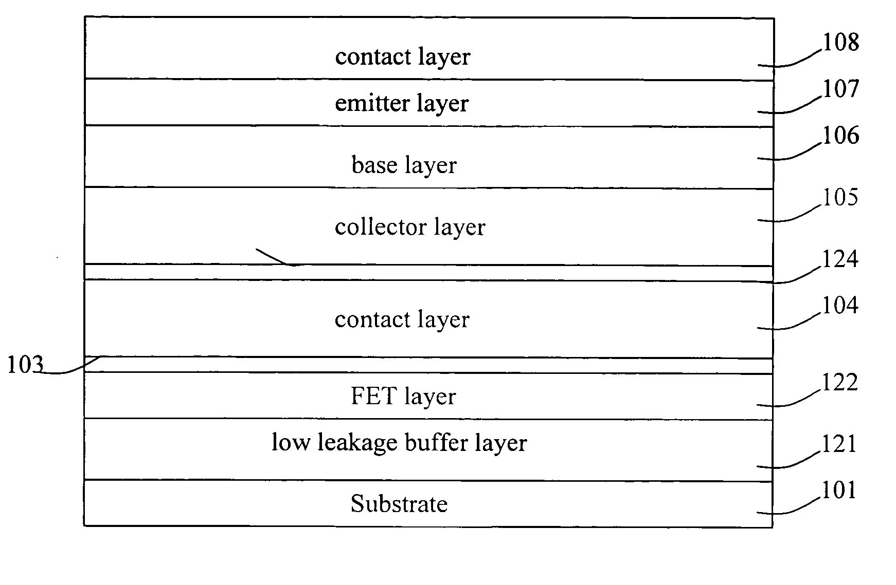
[0018]FIG. 1 illustrates the formation of the structure for fabricating an integrated FET and HBT pair in one embodiment of this invention. Substrate 101 is first provided and may be a semi-insulating GaAs wafer substrate, or any suitable substrate for fabricating the integrated HBT and FET pair. The GaAs substrate 101 may be fabricated using well-known crystal-growth technologies such as the Czochralski technique or the Bridgman technique. Detailed descriptions of these techniques can be found, for example, at page 343-349 of S. M. Sze, “Semiconductor Devices: Physics and Technology”, 2nd Ed., John Wiley & Sons, Inc. 2002.

[0019] After providing the substrate 101, a first epitaxial structure 102 may be grown on top of the substrate 101. The epitaxial structure 102 may comprise one or more epitaxial layers. The epitaxial structure 102 (and other epitaxial structures grown on top of it) may be fabricated using well-known technologies such as chemical vapor deposition (CVD), Metalorga...


PUM


Abstract

Methods and systems for fabricating integrated pairs of HBT / FET's are disclosed. One preferred embodiment comprises a method of fabricating an integrated pair of GaAs-based HBT and FET. The method comprises the steps of: growing a first set of epitaxial layers for fabricating the FET on a semi-insulating GaAs substrate; fabricating a highly doped thick GaAs layer serving as the cap layer for the FET and the subcollector layer for the HBT; and producing a second set of epitaxial layers for fabricating the HBT.

Description

FIELD OF INVENTION [0001] This invention is related in general to HBT / FET fabrication technologies and in particular to structures and methods for fabricating integrated InGaP / GaAs HBT / FET's on the same chip at a competitive cost. BACKGROUND OF INVENTION [0002] InGaP / GaAs HBT Technology is very attractive for use in many commercial applications for its excellent reliability and thermal stability. The first generation of InGaP-based power amplifiers for wireless handsets, wireless LAN, broadband gain blocks, and high-speed fiber optic products have been successfully developed and marketed. For future generations of these products, it is important to reduce the die size and cost as well as to provide additional functionality with improved circuit performance. The integration of bipolar (HBT) and field effect transistors (FET or HEMT) on the same chip offers a unique way to achieve these goals. While the combination of bipolar and field effect devices in an integrated circuit is well k...

Claims


Application Information

Patent Timeline
Patent Type & Authority Applications(United States)
IPC IPC(8): H01L27/06H01L29/739
CPCH01L27/0623H01L27/0605
Inventor KRUTKO, OLEHXIE, KEZHOUSHOKRANI, MOHSENGUPTA, ADITYAGEDZBERG, BORIS
Owner SKYWORKS SOLUTIONS INC
Why Eureka
Try Eureka