Display element, display device, and manufacturing method of display element

Active Publication Date: 2005-08-25
MERCK PATENT GMBH
View PDF5 Cites 56 Cited by
  • Summary
  • Abstract
  • Description
  • Claims
  • Application Information

AI Technical Summary

Benefits of technology

[0030] On the other hand, a conventional liquid crystal display element applies a field to a medium for display. In response to application of a field, the conventional liquid crystal display element causes no change in shape of refractive index ellipsoid but causes a change in direction of major axis of the ellipsoid. Specifically, the conventional display element uses the change in direction of major axis of ellipsoid, that occurs in response to application of a field, to realize varied display states. Accordingly, the display element of the present invention greatly differs in display principle from the conventional display element.
[0031] Thus, because the conventional liquid crystal display element utilizes the change in the alignment direction of liquid crystal molecules, the viscosity inherent in the liquid crystal has greatly affected the response speed. On the contrary, according to the foregoing arrangement, the change in degree of optical anisotropy in a medium is used for display. Therefore, according to the foregoing arrangement, unlike the conventional liquid crystal display element, there is little defect of the viscosity inherent in the liquid crystal that affects the response speed, thereby realizing high-speed response. Further, with this advantage of high-speed response, the display element according to the present embodiment is suitable for a display device using a field sequential color method or the like.
[0032] Further, a conventional liquid cryst

Problems solved by technology

However, the liquid crystal display adopting the TN mode has drawbacks in slow response and a narrow viewing angle.
Those disadvantages are large hindrances for the TN mode to take over CRT (Cathode Ray Tube).
The mode using the FLC or AFLC allows high-speed response and wide viewing angle, but has drawbacks in shock resistance and temperature characteristics.
This prevents wide and practical application of the mode using the FLC or AFLC.
However, in the polymer dispersed liquid crystal display mode, it is intrinsically impossible to control the viewing angle with the use of a phase plate.
Further, the polymer dispersed liquid crystal display mode has a problem in its response property.
Although the mode using the FLC or AFLC has advantages in its response speed and its viewing angle, the mode has a problem of irreversible alignment breakdown due to external force.
However, one of the problems in practically employing the Kerr effect for a display element is driving voltage that is greater than that for driving a conventional liquid crystal display element.
However, the art disclosed in the foregoing publication has a problem in that the region in which the Kerr effect can be easily generated is limited to a vicinity of surfaces of the substrate.
Therefore, the art of the foregoing technique provides only little reduction of the driv

Method used


Image

  • Display element, display device, and manufacturing method of display element
  • Display element, display device, and manufacturing method of display element
  • Display element, display device, and manufacturing method of display element

Examples


first embodiment

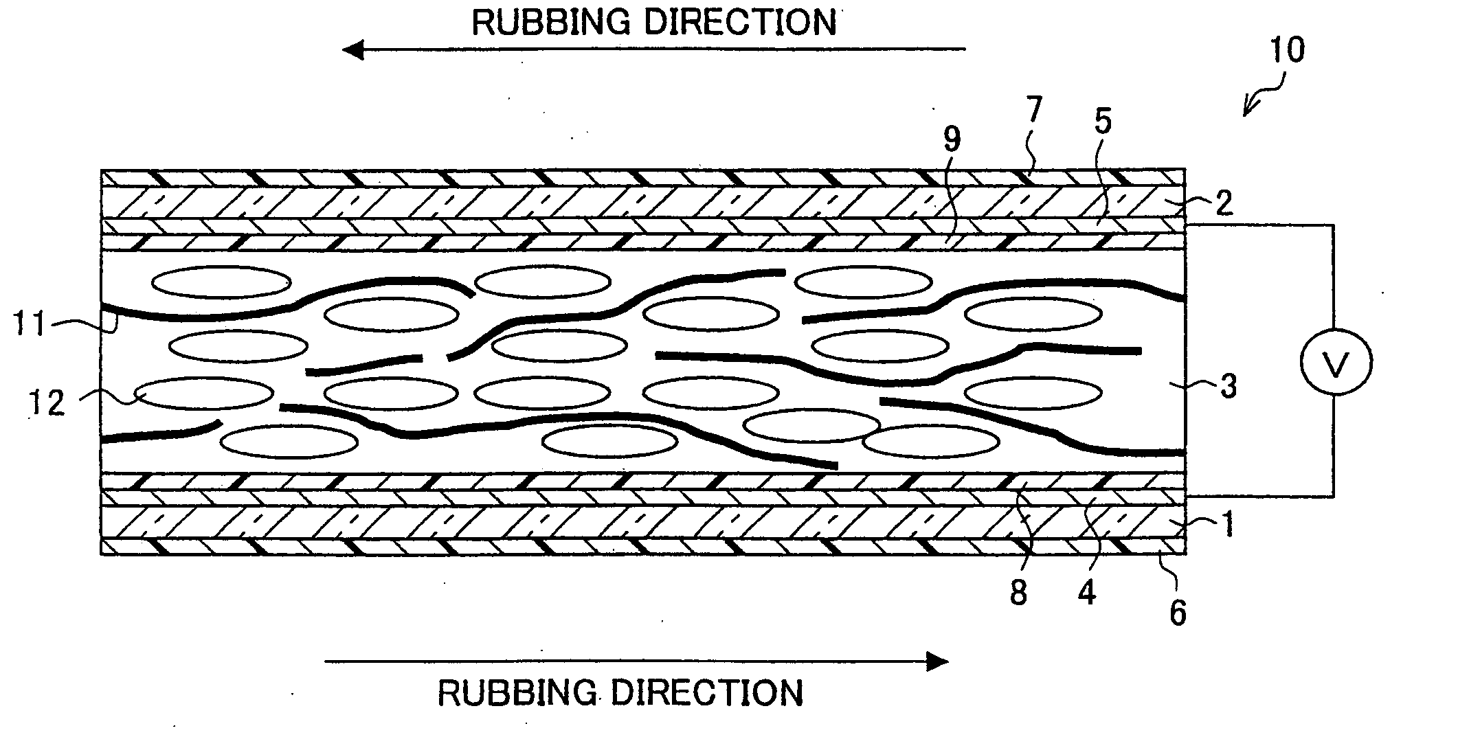
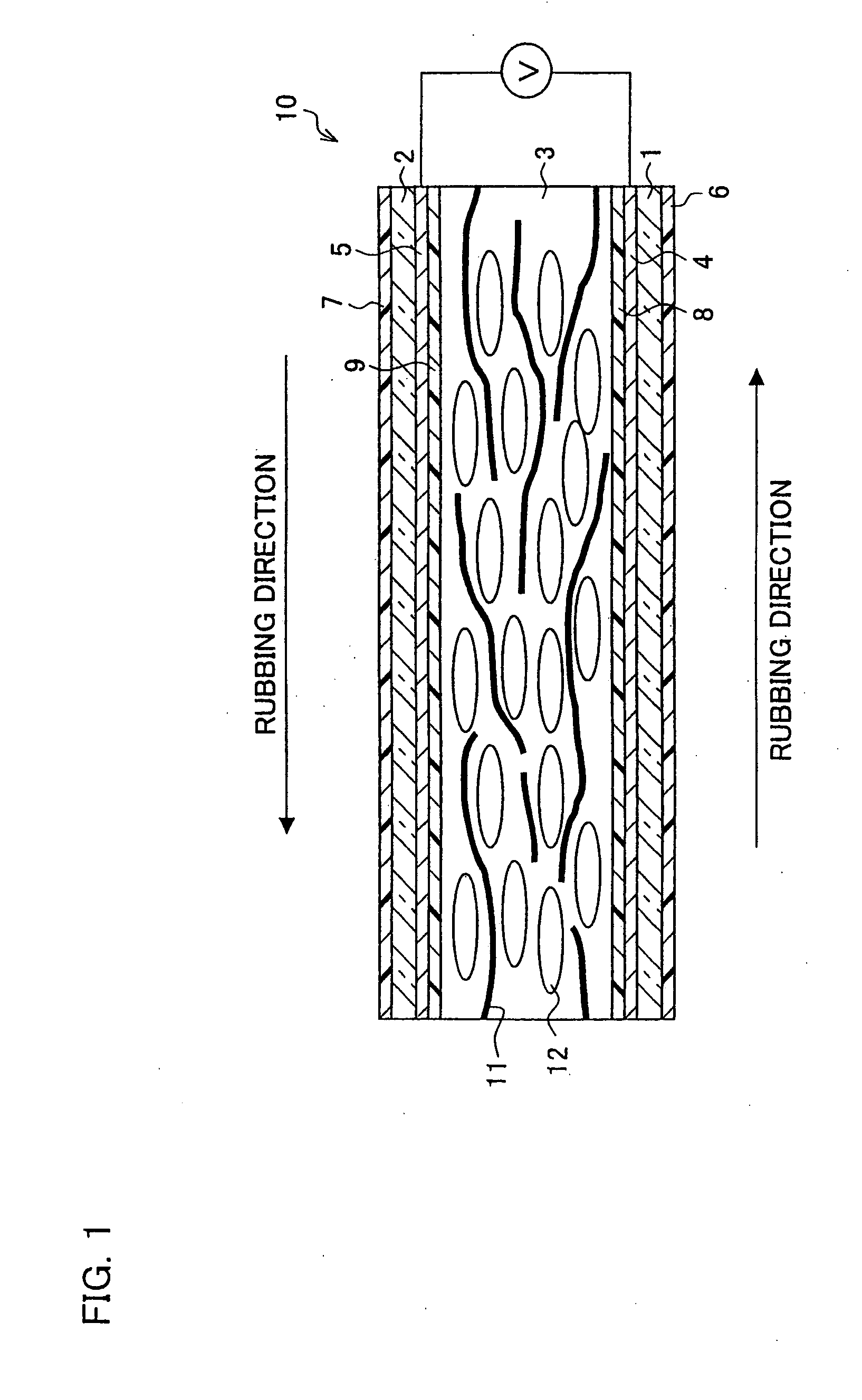
[0069] An embodiment of the present invention is described below, referring to Figures. Note that, the respective embodiments in this specification mainly deal with the case of using a field as means for changing degree of optical isotropy of the medium; however, the present invention is not limited to this case, and a magnetic field, light etc. may be used instead of a field. Further, the present embodiment mainly deals with the case of carrying out display with a medium that exhibits an optical isotropy when a field (external field) is applied or when no electrical field (external field) is applied; however, the present invention is not limited to this case. More specifically, the medium of the present embodiment is not limited to the medium that is isotropic when a field (external field) is applied or when no field (external field) is applied, but may be a medium that is anisotropic when no field (external field) is applied, and is changed in degree of optical anisotropy in respo...

second embodiment

[0188] The following explains another embodiment of the present invention with reference to Figures. For ease of explanation, materials having the equivalent functions as those shown in the drawings pertaining to the foregoing First Embodiment will be given the same reference symbols, and explanation thereof will be omitted here.

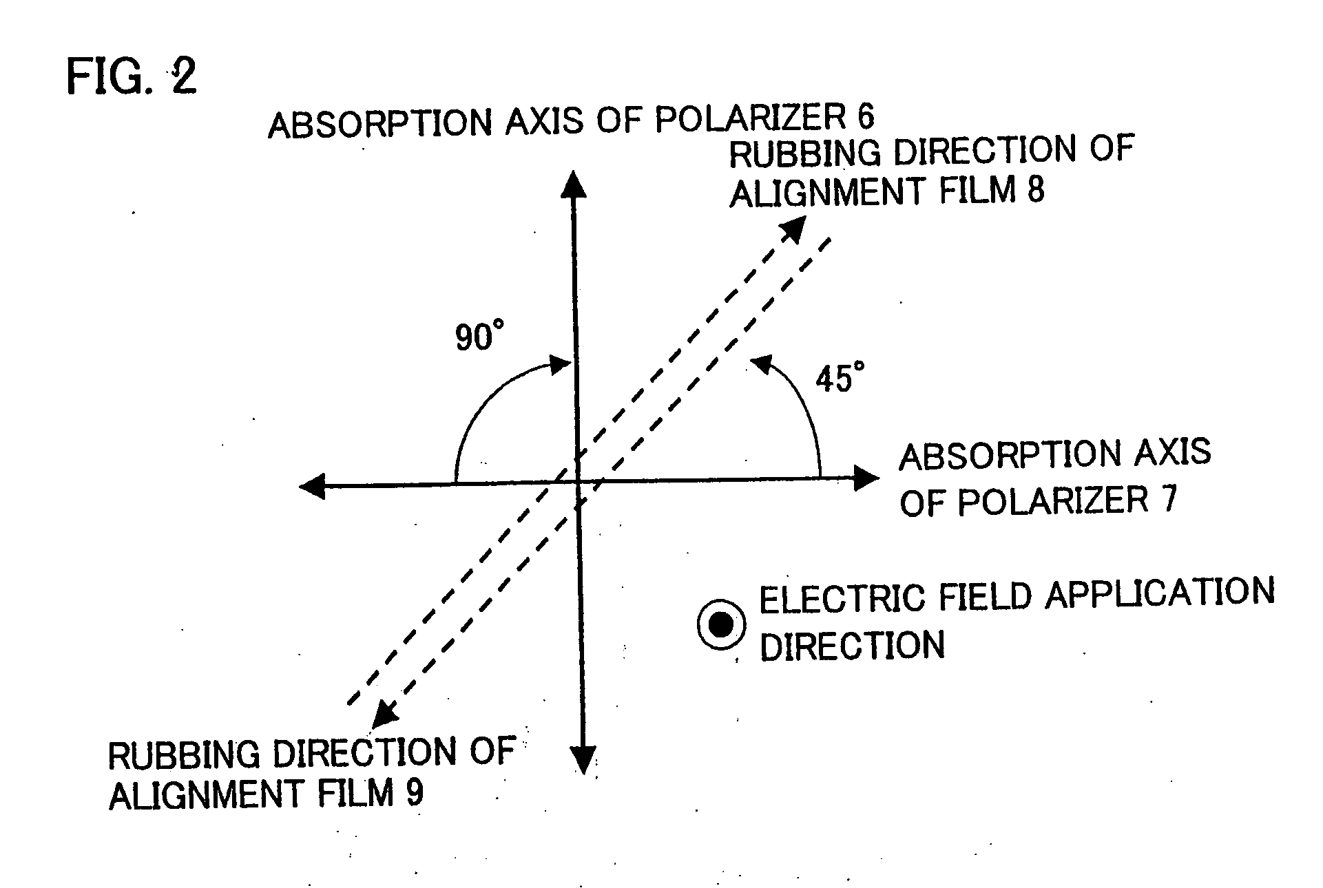
[0189] The present embodiment also uses the display element described in First Embodiment, which however includes the alignment films 8 and 9 that differ from each other in rubbing directions. More specifically, the display element of the present embodiment has the same structure as that of the display element of First Embodiment except for the alignment films 8 and 9 that differ from each other in rubbing directions. Note that, as to the medium to be sealed in the material layer 3, the display element of the present embodiment uses the medium with negative dielectric anisotropy, that is one of the mediums described in First Embodiment. Further, the display...

third embodiment

[0212] The following explains still another embodiment of the present invention with reference to Figures. For ease of explanation, materials having the equivalent functions as those shown in the drawings pertaining to the foregoing First Embodiment will be given the same reference symbols, and explanation thereof will be omitted here.

[0213]FIG. 13 is a cross-sectional view illustrating a schematic structure of a display element (display element 30) according to the present embodiment. For example, the display element 30 is provided in the display device 100 as a replacement of the display element of First Embodiment. As shown in the figure, the display element 30 includes a material layer (optical modulation layer) 3 between the two opposed substrates (substrate 1 and substrate 2). Further, on one surface of the substrate 1, the surface opposite to the substrate 2, pectination electrodes (pectination-shaped electrodes) 4a and 5a, that function as field applying means for applying ...


PUM

PropertyMeasurementUnit
Wavelengthaaaaaaaaaa
Particle diameteraaaaaaaaaa
Temperatureaaaaaaaaaa

Abstract

Each of a pair of substrates respectively comprises an electrode and a rubbed alignment film on one surface, while the other surface is provided with a polarizer. The substrates are placed so that the surfaces provided with the alignment films are opposed to each other, and the area between the substrates is filled with a medium to form a material layer. Then, a medium made of a negative-type liquid crystalline compound sing a photopolymerizable monomer and a polymerization initiator is injected into the material layer held between the substrates. Further, ultra violet irradiation is performed with the medium exhibiting a liquid crystal phase, so that the photopolymerized monomer is polymerized, thus forming a polymer chain. In this manner, obtained is a display element, that causes change in degree of optical anisotropy in response to application of electric (external) field, which display element can be driven by a lower intensity electric (external) field.

Description

[0001] This Nonprovisional application claims priority under 35 U.S.C. § 119(a) on Patent Application No. 2004 / 008444 filed in Japan on Jan. 15, 2004, No. 2004 / 253425 filed Japan on Aug. 31, 2004, and No. 2005 / 007497 filed in Japan on Jan. 14, 2005, the entire contents of which are hereby incorporated by reference. FIELD OF THE INVENTION [0002] The present invention relates to a display element and a display device with high speed response and wide viewing angle, which display element and device can be driven by a low-intensity external field. The present invention also relates to a manufacturing method of the display element. BACK GROUND OF THE INVENTION [0003] A liquid crystal display element has advantages over other display element in terms of thinness, lightness in weight, and small power consumption, and is therefore widely used for image display devices such as a television and a monitor, and image display devices provided on: OA (Office Automation) equipments such as a word ...

Claims


Application Information

Patent Timeline
IPC IPC(8): C09K19/00G02F1/1333C09K19/02C09K19/42C09K19/58G02F1/07G02F1/133G02F1/137G09G3/36
CPCC09K19/02C09K19/586C09K2019/0418G02F2001/13775G02F1/07G02F1/13718C09K2019/0492G02F1/13775G02F1/1333C09K19/42
Inventor MIYACHI, KOICHISHIBAHARA, SEIJIINOUE, IICHIROISHIHARA, SHOICHIKOIDE, TAKAKO
Owner MERCK PATENT GMBH
Why Eureka
Try Eureka