Process for manufacturing photovoltaic cells

a photovoltaic cell and manufacturing technology, applied in the direction of manufacturing tools, sustainable manufacturing/processing, final product manufacturing, etc., can solve the problems of reducing the efficiency of the cell, affecting the formation of the back surface field, and unfavorable cell efficiency reduction

Inactive Publication Date: 2005-09-01
BP CORP NORTH AMERICA INC
View PDF13 Cites 48 Cited by
  • Summary
  • Abstract
  • Description
  • Claims
  • Application Information

AI Technical Summary

Problems solved by technology

However, these are not the only methods use to obtain suitable semiconductor wafers for the manufacture of photovoltaic devices and particularly photovoltaic cells.
If the front contact is too large in area, the amount of shading caused by the opaque contact itself will reduce the amount of light impinging on the cell and result in the undesirable reduction of cell efficiency.
For example, in the process described above it is believed that the n-type dopant, such as phosphorus, applied to and diffused into the grooves cut into the wafer, also diffuses into the rear surface of the wafer thereby adversely affecting the formation of the back surface field and resulting in a reduction of the efficiency of the cell.

Method used


Image

  • Process for manufacturing photovoltaic cells
  • Process for manufacturing photovoltaic cells

Examples


examples 1 and 2

OF THE INVENTION

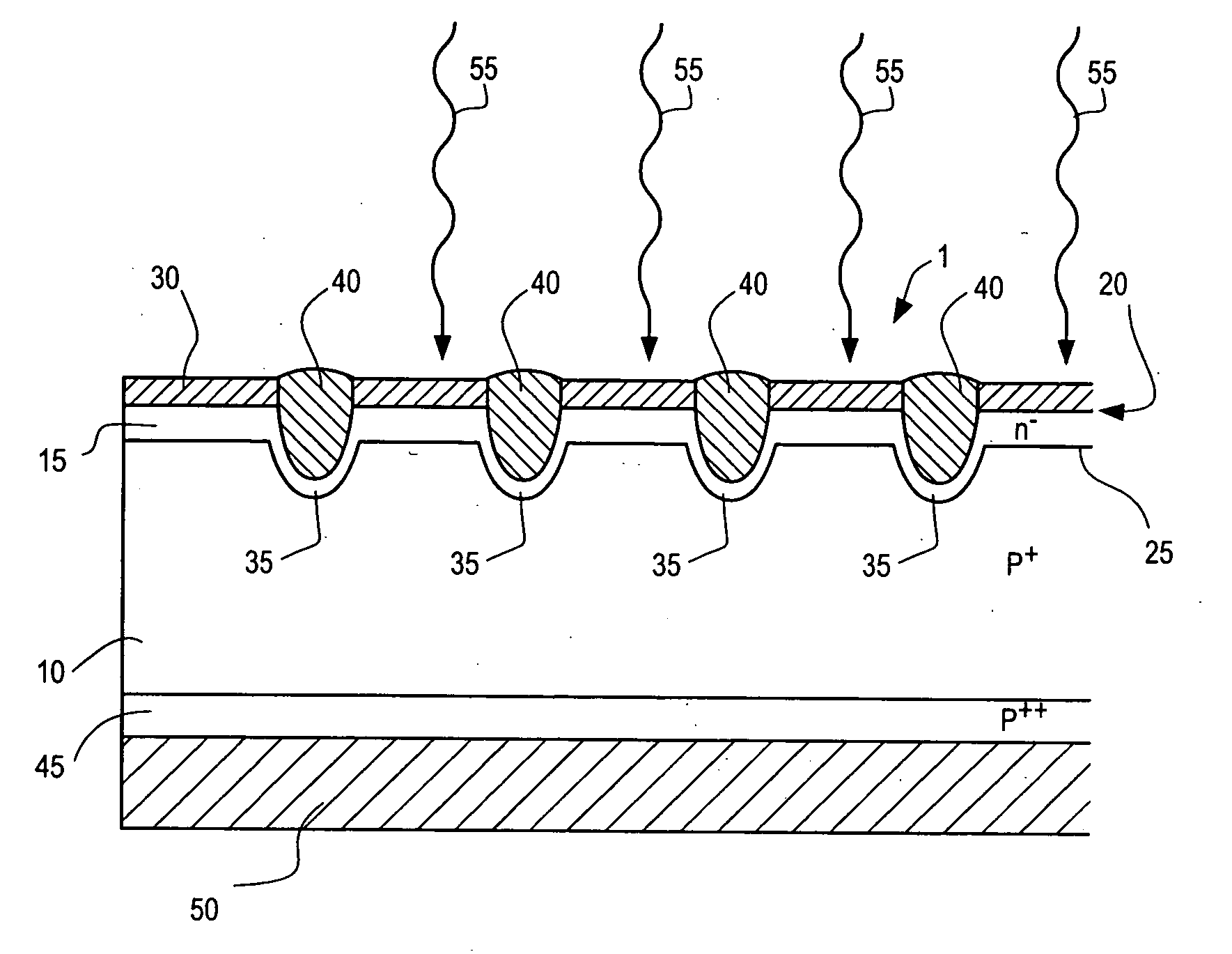
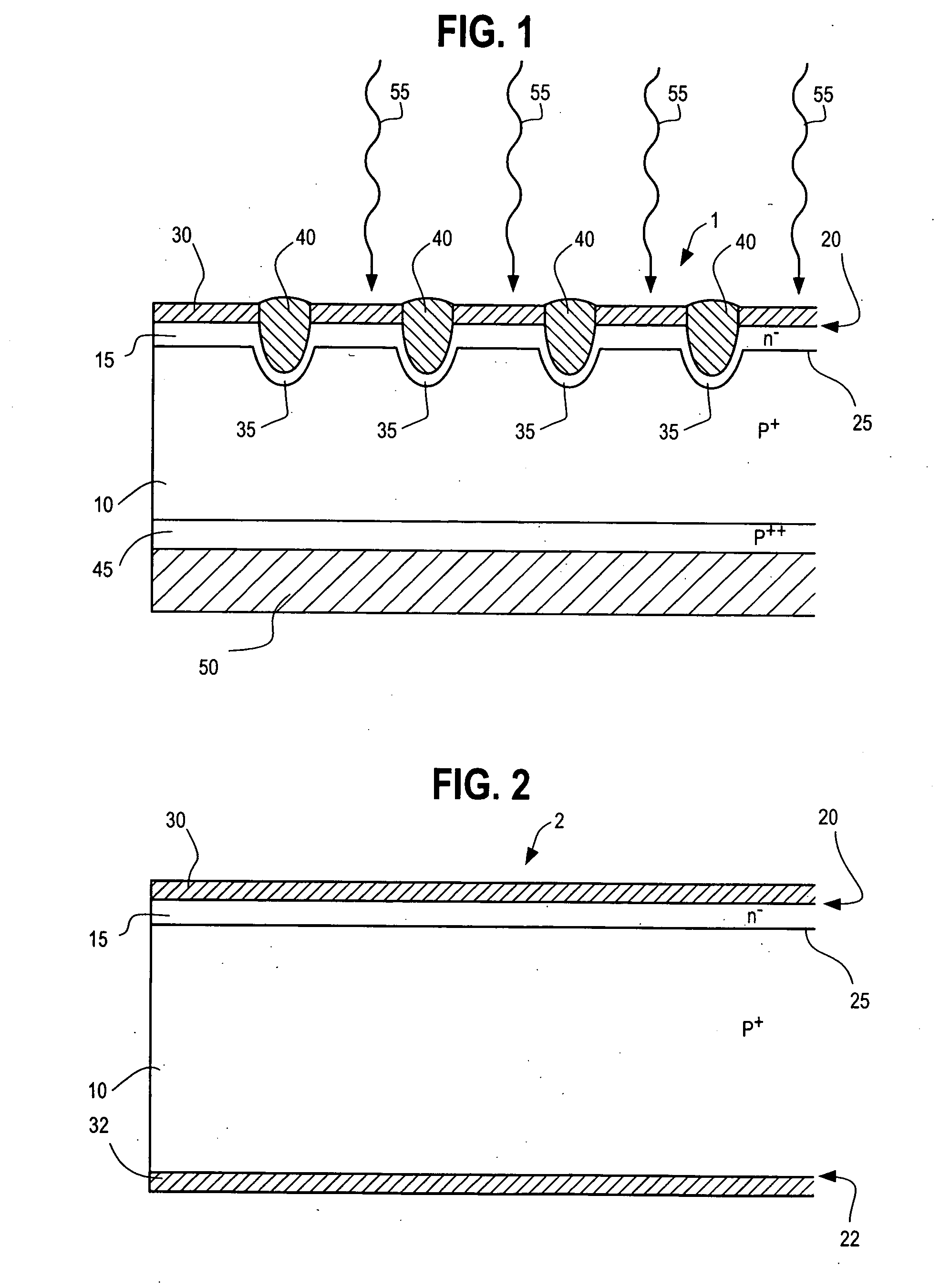
[0037] Examples 1 and 2 are examples of solar cells having an area of 147 cm2 that were prepared using the general process and in the order of process steps in accordance with this invention as follows:

[0038] 1. Starting Material

[0039] The silicon wafers used were conventional Cz silicon wafers doped p-type with boron to a resistivity of 1.2 ohm.cm and grown with [100] crystal planes parallel to the wafer surface. The wafer dimensions were 127 millimeters square with rounded corners of a diameter 150 millimeters. The wafer thickness was 300 micrometers. Such wafers are commercially available, for example, from Bayer Solar GmbH, PV Silicon GmbH or Pillar.

[0040] 2. Wafer Surface Preparation

[0041] The wafers were anisotropically “texture” etched in a solution of sodium hydroxide and propanol at a temperature of 90° C. and cleaned by subsequent immersions in hydrofluoric acid and hydrochloric acid with intermediate and final rinsing in de-ionized water followed by dr...


PUM

PropertyMeasurementUnit
thickaaaaaaaaaa
thickaaaaaaaaaa
diameteraaaaaaaaaa

Abstract

A process for making a photovoltaic cell using a semiconductor wafer doped with a first dopant and having a front surface and a back surface, the process comprising the steps of forming a first layer on the front surface of the wafer, the first layer comprising a second dopant of a conductivity type opposite the first dopant; depositing a surface coating on the back surface; forming grooves in the front surface; adding dopant to the groove of a conductivity type opposite the first dopant subsequent to depositing the surface coating on the back surface; removing the surface coating from the back surface after adding dopant to the grooves; forming a back contact over the back surface after removal of the surface coating; and adding conductive material to the grooves.

Description

[0001] This application claims the benefit of U.S. Provisional Patent Application No. 60 / 532,268, filed on Dec. 23, 2003.BACKGROUND OF THE INVENTION [0002] This invention relates to a process for manufacturing photovoltaic cells. More particularly, this invention relates to a process useful for manufacturing photovoltaic cells that are highly efficient in converting light energy, and particularly solar energy, to electrical energy. One of the most important features of a photovoltaic cell is its efficiency in converting light energy from the sun into electrical energy. Thus, the art is continuously striving to not only reduce the cost of manufacturing photovoltaic cells, but also to improve their efficiency in converting light energy into electrical energy. This invention also relates to highly efficient solar cells and semiconductor wafers that can be used to manufacture highly efficient solar cells. [0003] Typically, a plurality of photovoltaic cells are arranged in one or more pa...

Claims


Application Information

Patent Timeline
Patent Type & Authority Applications(United States)
IPC IPC(8): H01L31/00H01L31/0224H01L31/068H01L31/18
CPCB23K26/367H01L31/022425Y02E10/547H01L31/1804H01L31/068B23K26/364Y02P70/50
Inventor HARTLEY, OLIVER
Owner BP CORP NORTH AMERICA INC
Why Eureka
Try Eureka