Super bright light emitting diode of nanorod array structure having InGaN quantum well and method for manufacturing the same

a technology of light-emitting diodes and nanorod arrays, which is applied in the direction of material nanotechnology, semiconductor devices, semiconductor/solid-state device details, etc., can solve the problems of high coefficient of thermal expansion, poor light-emitting efficiency, and limited element performance of laminated-film leds, etc., and achieve good yield and high light-emitting efficiency

Active Publication Date: 2005-09-08
DONGGUK UNIV IND ACADEMIC COOPERATION FOUND
View PDF10 Cites 130 Cited by
  • Summary
  • Abstract
  • Description
  • Claims
  • Application Information

AI Technical Summary

Benefits of technology

[0008] In addition, an object of the invention is to provide a method for reproducibly manufacturing the GaN LED having super brightness and high light emission efficiency.
[0014] According to the present invention, it is possible to obtain an LED having great-brightness and high light emission efficiency at a good yield without any catalyst or template.

Problems solved by technology

However, GaN currently uses a sapphire substrate since there is no lattice-matched substrate at present, so there is still much mismatching and coefficient of thermal expansion is still great.
However, the laminated-film LED has a limit in the element performance (or, brightness) since many threading dislocations exist due to the lattice mismatching, caused by the aforementioned properties and growth manners of GaN.
In addition, the conventional laminated-film GaN LED suffers from some limitations such as the poor extraction efficiency of light, the wide spectral width, and the large divergence of the output as well as the aforementioned threading dislocations, in spite of many advantages of being relatively simple to design and manufacture and having low temperature sensitivity.
However, there is unfortunately found that many threading dislocations are generated in such a nano-scale or micro-scale LED similar to the laminated-film LED, so an LED having super brightness to a satisfactory level is not still appeared.
In addition, the nanorod LED is a simple p-n junction diode, not giving super brightness.
Moreover, the micro-ring or micro-disc LED is currently manufactured using photolithography or electron-beam lithography which is apt to damage the lattice structure of GaN during the lithography process, so brightness and light emission efficiency of the LED are not satisfactory.

Method used


Image

  • Super bright light emitting diode of nanorod array structure having InGaN quantum well and method for manufacturing the same
  • Super bright light emitting diode of nanorod array structure having InGaN quantum well and method for manufacturing the same
  • Super bright light emitting diode of nanorod array structure having InGaN quantum well and method for manufacturing the same

Examples


Embodiment Construction

[0027] Hereinafter, preferred embodiments of the present invention will be described in detail referring to the accompanying drawings. Prior to the description, it should be understood that the terms used in the specification and appended claims should not be construed as limited to general and dictionary meanings, but interpreted based on the meanings and concepts corresponding to technical aspects of the present invention on the basis of the principle that the inventor is allowed to define terms appropriately for the best explanation. Therefore, the description proposed herein is just a preferable example for the purpose of illustrations only, not intended to limit the scope of the invention, so it should be understood that other equivalents and modifications could be made thereto without departing from the spirit and scope of the invention.

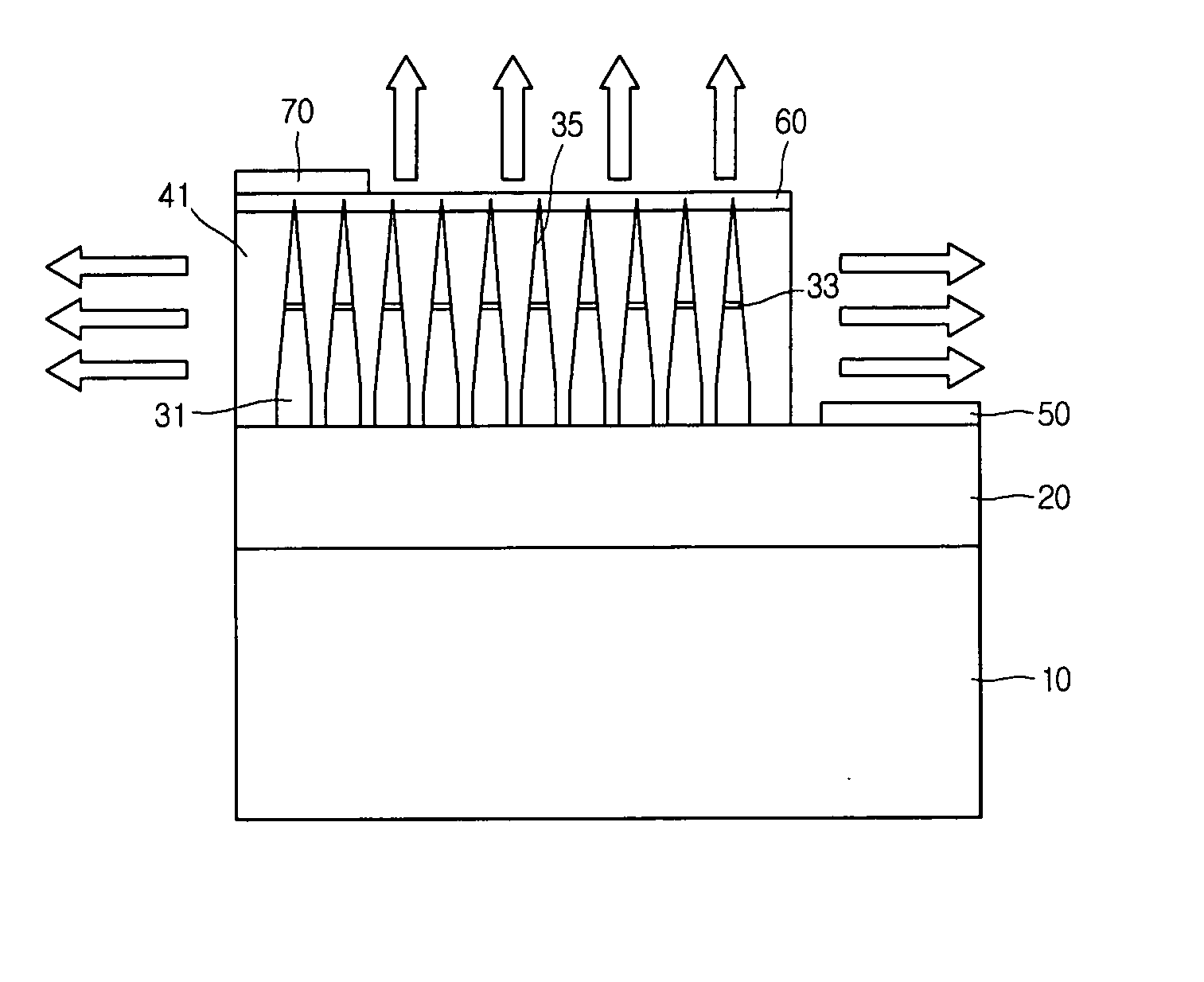
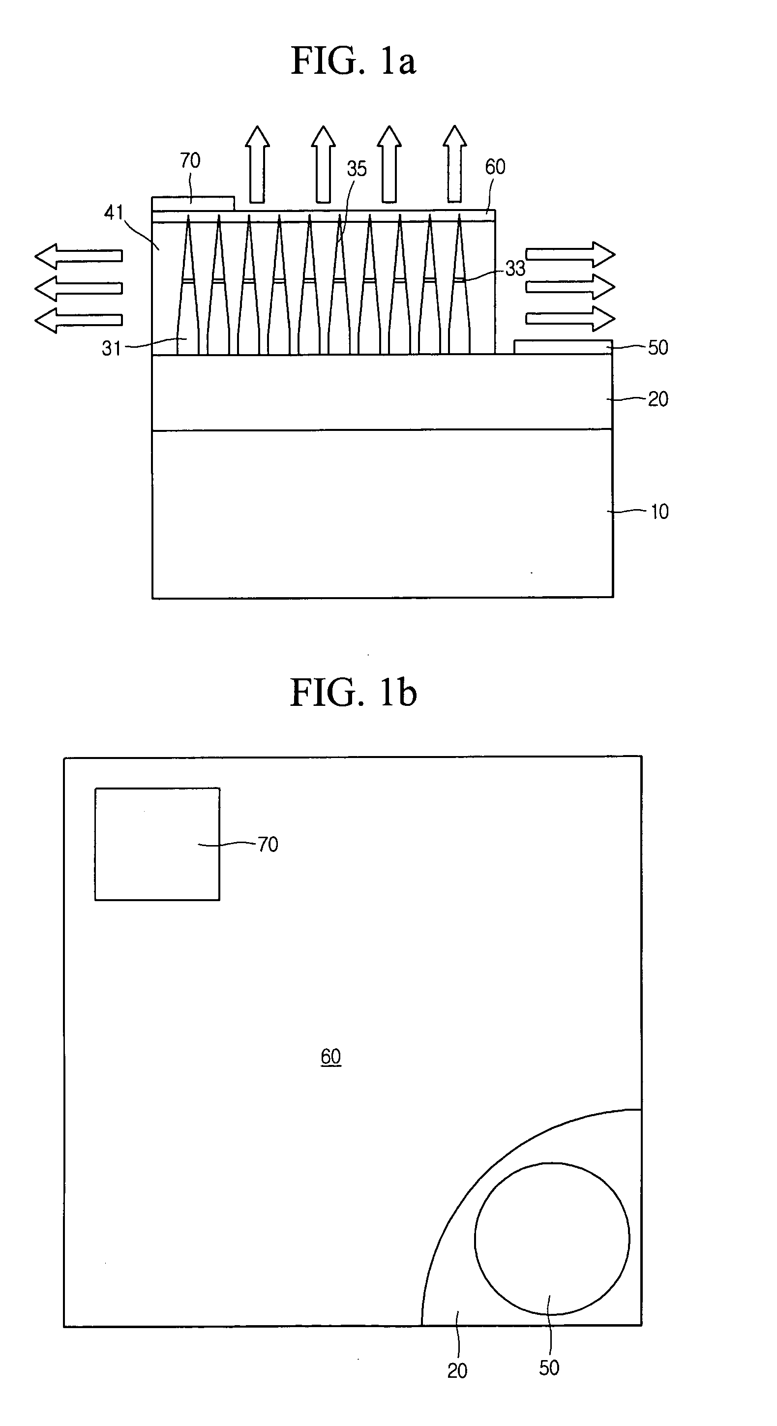
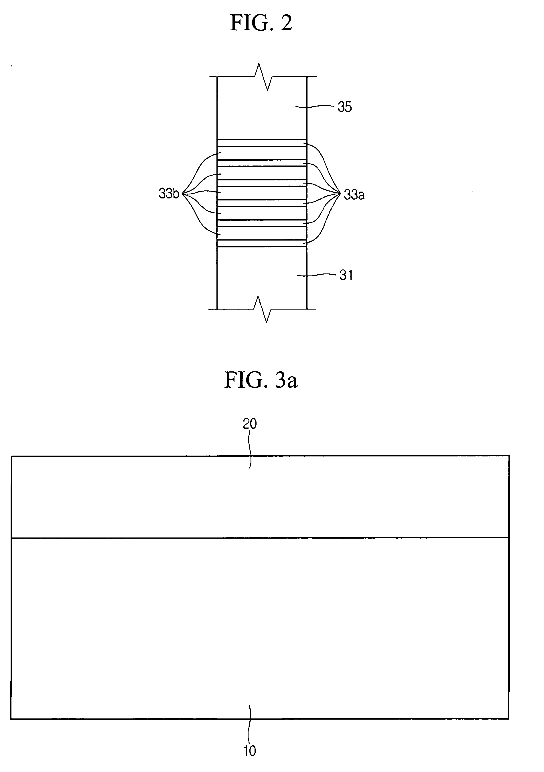
[0028]FIG. 1a is a schematic view showing a section of a light emitting diode (LED) according to a preferred embodiment of the present invent...


PUM


Abstract

An GaN light emitting diode (LED) having a nanorod (or, nanowire) structure is disclosed. The GaN LED employs GaN nanorods in which a n-type GaN nanorod, an InGaN quantum well and a p-type GaN nanorod are subsequently formed in a longitudinal direction by inserting the InGaN quantum well into a p-n junction interface of the p-n junction GaN nanorod. In addition, a plurality of such GaN nanorods are arranged in an array so as to provide an LED having much greater brightness and higher light emission efficiency than a conventional laminated-film GaN LED.

Description

BACKGROUND OF THE INVENTION [0001] 1. Field of the Invention [0002] The present invention relates to a super bright light emitting diode (LED), and more particularly to an LED having a nanorod (or, nanowire) structure and its manufacturing method. [0003] 2. Description of the Related Art [0004] LED is generally used as a simple display element of a gauge or meter at the early state, and recently noticed as a full-color display element having super brightness, high contrast and long life cycle owing to the development of blue and green super brightness LED. On the other hand, as a material of such an LED, a III-nitrogen compound semiconductor using such as GaN is recently researched abundantly since III-V group nitride semiconductors have so wide a bandgap to give a light in the almost all wavelengths from visible rays to ultraviolet rays according to composition of nitride. However, GaN currently uses a sapphire substrate since there is no lattice-matched substrate at present, so th...

Claims


Application Information

Patent Timeline
Patent Type & Authority Applications(United States)
IPC IPC(8): H01L27/15
CPCB82Y30/00H01L33/08H01L33/18H01L33/32Y10S977/762Y10S438/962Y10S977/764Y10S977/815Y10S438/979Y10S977/765Y10S977/825Y10S977/784Y10S977/763
Inventor KIM, HWA-MOKKANG, TAE-WONCHUNG, KWAN-SOO
Owner DONGGUK UNIV IND ACADEMIC COOPERATION FOUND
Why Eureka
Try Eureka