Submount and semiconductor device

a semiconductor device and sub-mount technology, applied in the direction of semiconductor lasers, soldering devices, manufacturing tools, etc., can solve the problems of reduced density of solder layers, preventing adequate improvement of bonding strength, and density greater than 99.9% of theoretical density,

Active Publication Date: 2005-09-08
SUMITOMO ELECTRIC IND LTD
View PDF10 Cites 31 Cited by
  • Summary
  • Abstract
  • Description
  • Claims
  • Application Information

AI Technical Summary

Benefits of technology

[0007] The object of the present invention is to overcome the problems described above and to provide a submount capable of

Problems solved by technology

If the density of the solder layer is less than 50% of the theoretical density, the reduced density of the solder layer prevent

Method used


Image

  • Submount and semiconductor device
  • Submount and semiconductor device
  • Submount and semiconductor device

Examples


first embodiment

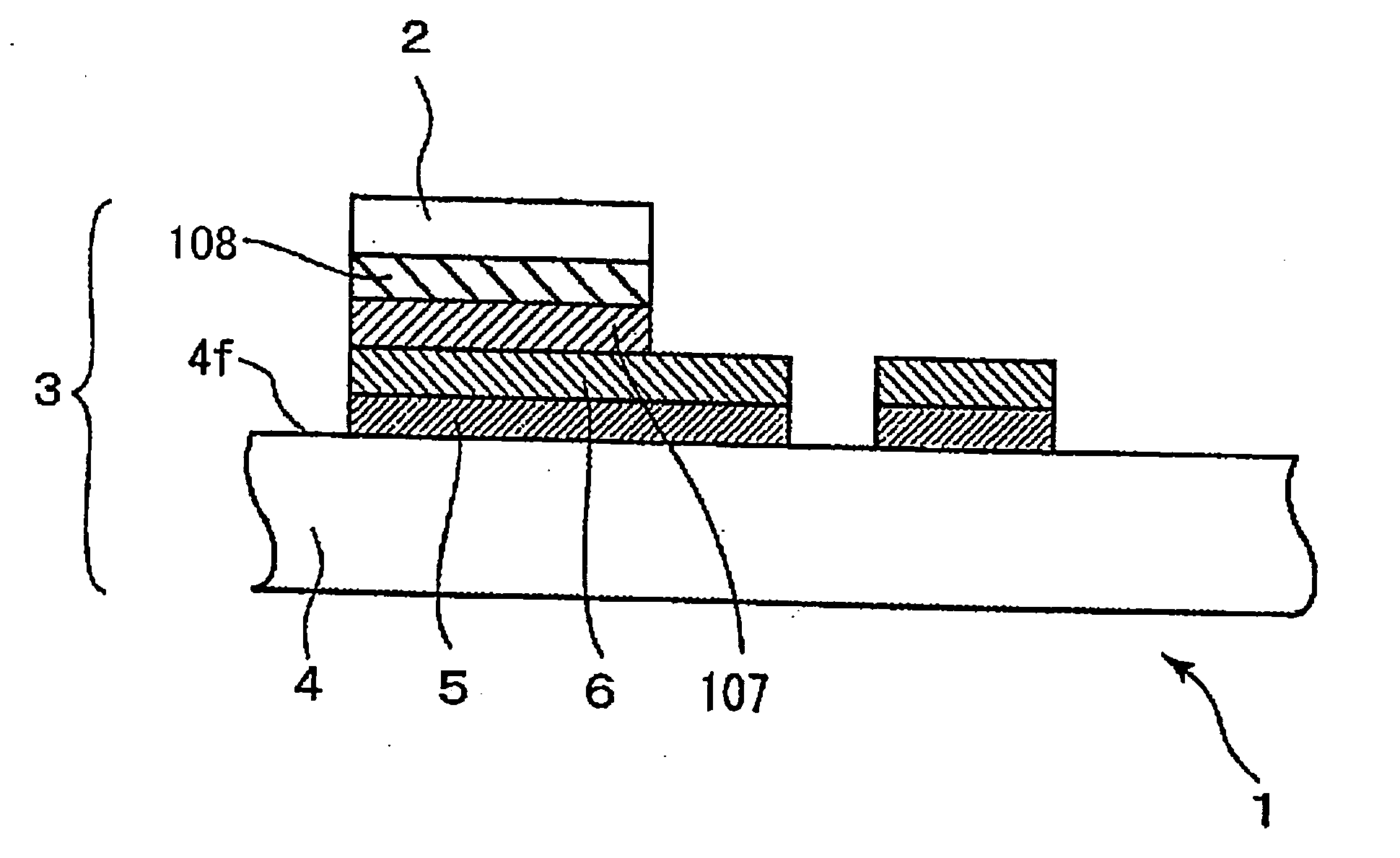
[0027] An embodiment of the present invention will be described, with references to the figures. Elements that are identical or correspond to each other in these figures are assigned the same numerals and overlapping descriptions will be omitted. FIG. 1 shows a simplified cross-section drawing of a semiconductor device according to the first embodiment of the present invention. As shown in FIG. 1, the semiconductor device 1 is equipped with: a submount 3; and a laser diode 2, serving as a semiconductor light-emitting element, mounted on the submount 3 via a solder layer 8. The solder layer 8 has a density of at least 50% and no more than 99.9% of the theoretical density of the AuSn-based solder used in the solder layer 8.

[0028] The submount 3 is formed by layering the following onto a substrate 4: a Ti / Pt layered film 5; a gold (Au) film 6; a solder barrier layer 107; and a solder layer 8. The semiconductor device shown in FIG. 1 is made by first preparing the submount 3 onto which...

second embodiment

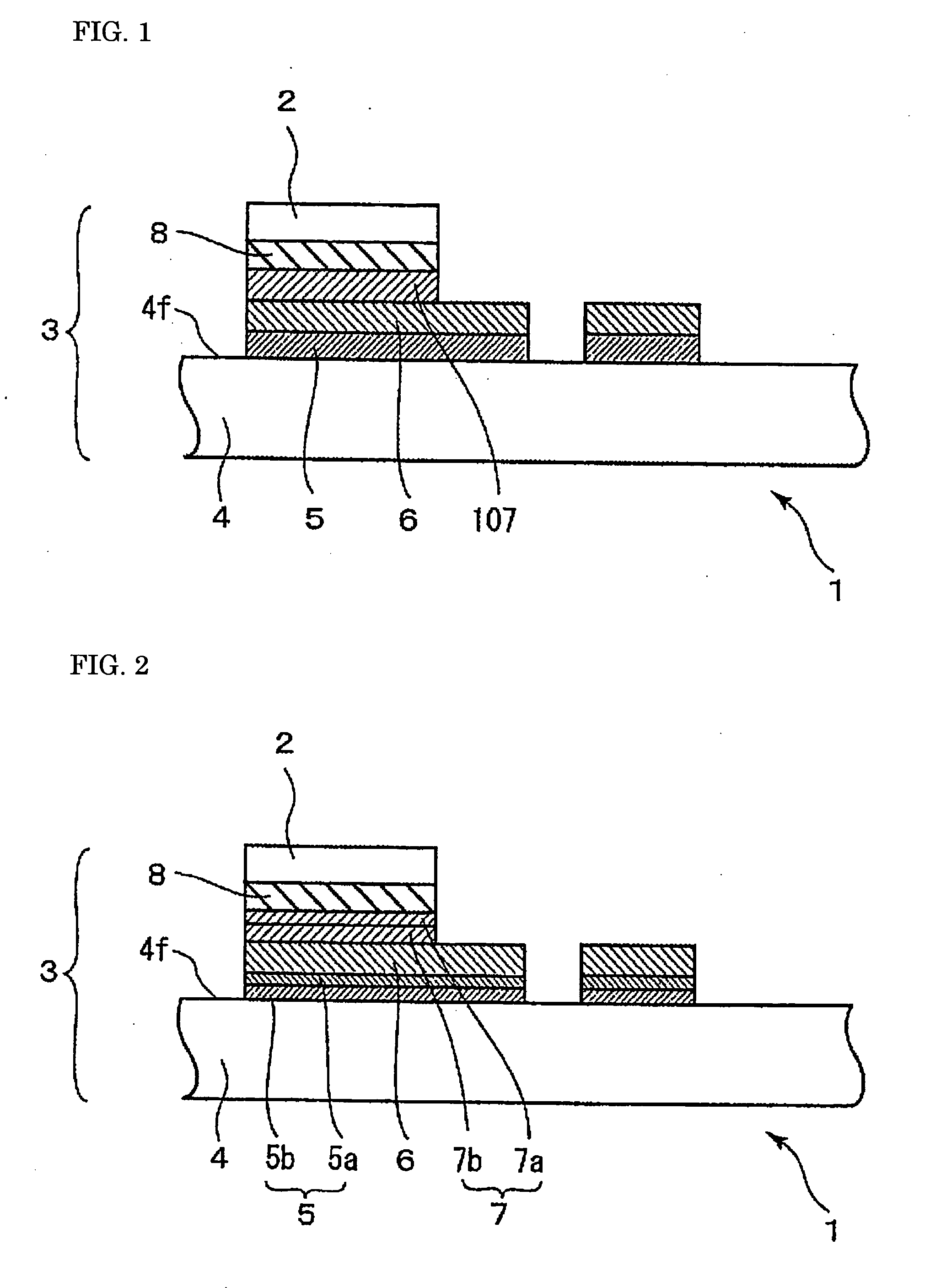
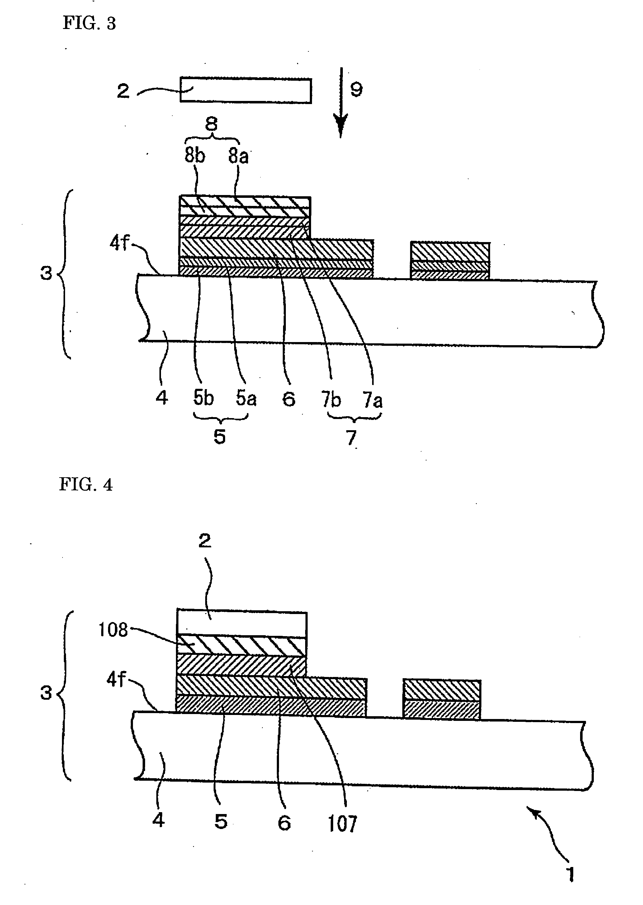
[0033]FIG. 2 shows a simplified cross-section drawing of a semiconductor device according to a second embodiment of the present invention. FIG. 3 is a simplified cross-section drawing for the purpose of describing how the semiconductor device shown in FIG. 2 is made, and shows the state before solder is melted.

[0034] As shown in FIG. 2, the semiconductor device 1 is formed as a structure wherein a laser diode 2 serving as a semiconductor light-emitting element is mounted onto a submount 3. The submount is formed from: a submount substrate 4 formed from a material such as sintered aluminum nitride (AlN); a layered film 5 (Ti / Pt layered film 5) formed from a titanium (Ti) film 5b serving as an adhesion layer and a platinum (Pt) film 5a serving as a diffusion barrier layer; a gold (Au) film 6 formed on the Ti / Pt layered film 5 and serving as an electrode layer; and a solder adhesion layer 7 formed from a titanium (Ti) film 7b serving as a transition element layer and a platinum (Pt) f...

embodiment

(Making and Evaluating Samples)

[0067] Based on the method described above, submounts were made from sample 1 through sample 11 indicated in Table 1. Samples 2 through 11 correspond to embodiments and sample 1 corresponds to a comparative example.

TABLE 1Solder LayerSolderSolderSolderfilm-Laser diodecompositionSolder filmrelativeformationDie ShearSampleratio (massthicknessdensityrateBondingstrengthNumberSubstrateratio)(microns)(%)(nm / s)temperature(MPa)1SinteredAg:Sn = 32:681.5 / 4.042125037AIN(layered Ag / Sn)2SinteredAg:Sn = 32:681.5 / 4.0621.525047AIN(layered Ag / Sn)3SinteredAg:Sn = 32:681.5 / 4.099225052AIN(layered Ag / Sn)4SinteredAg:Sn = 32:681.5 / 4.092525051AIN(layered Ag / Sn)5SinteredAg:Sn = 32:681.5 / 4.088925050AIN(layered Ag / Sn)6SinteredAg:Sn = 32:681.5 / 4.094225049SiC(layered Ag / Sn)7SinteredAg:Sn = 32:681.5 / 4.095225047Al2O3(layered Ag / Sn)8CuWAg:Sn = 32:681.5 / 4.097225048(layered Ag / Sn)9SinteredAg:Sn = 10:903.5 (alloy)96225049AIN10SinteredAu:Sn = 80:203.5 (alloy)93228547AIN11SinteredAu:S...


PUM

PropertyMeasurementUnit
Fractionaaaaaaaaaa
Fractionaaaaaaaaaa
Densityaaaaaaaaaa

Abstract

The present invention provides a submount that allows a semiconductor light-emitting element to be attached with a high bonding strength.
A submount 3 is equipped with a substrate 3 and a solder layer 8 formed on a primary surface 4f of the substrate 4. The density of the solder layer 8 is at least 50% and no more than 99.9% of the theoretical density of the material used in the solder layer 8. The solder layer 8 contains at least one of the following list: gold-tin alloy; silver-tin alloy; and lead-tin alloy. The solder layer 8 before it is melted is formed on the substrate 4 and includes an Ag film 8b and an Sn film 8a formed on the Ag film 8b. The submount 3 further includes an Au film 6 formed between the substrate 4 and the solder layer 8.

Description

TECHNICAL FIELD [0001] The present invention relates to a submount and semiconductor device that uses the same. More specifically, the present invention relates to a submount on which a semiconductor light-emitting element is mounted and a semiconductor device that uses this submount. In the present invention, a “semiconductor light-emitting element” refers to an element such as a laser diode or a light-emitting diode. BACKGROUND ART [0002] Semiconductor devices equipped with semiconductor light-emitting elements are widely known. One of these types of semiconductor devices, shown in FIG. 4, is made by mounting a semiconductor light-emitting element in a submount 3. FIG. 4 is a simplified cross-section drawing illustrating how the conventional semiconductor device is made. The conventional method for making the semiconductor device will be described, with references to FIG. 4. [0003] As shown in FIG. 4, in the conventional method for making a semiconductor device 1, the submount 3 i...

Claims


Application Information

Patent Timeline
IPC IPC(8): H01L21/60H01L21/52H01S5/02H01S5/022
CPCB23K1/0016B23K1/19B23K35/0238B23K35/262B23K35/268B23K35/3006B23K35/3013B23K2201/40B32B15/01B32B15/018H01L24/83H01L2224/13111H01L2224/8319H01L2224/83801H01L2924/01004H01L2924/01005H01L2924/01013H01L2924/01015H01L2924/01029H01L2924/01032H01L2924/01033H01L2924/0104H01L2924/01042H01L2924/01046H01L2924/01047H01L2924/01049H01L2924/0105H01L2924/01073H01L2924/01074H01L2924/01078H01L2924/01079H01L2924/01082H01L2924/01088H01L2924/10329H01S5/02272H01L24/29H01L24/32H01L2924/01006H01L2924/01019H01L2924/01023H01L2924/01024H01L2924/01041H01L2924/014H01L2924/0132H01L2924/15787H01L2224/29109H01L2224/29111H01L2924/12041H01L2924/01028H01L2924/00014H01L2924/12042B23K2101/40H01S5/0237H01L2924/00H01L2224/0401
Inventor ISHII, TAKASHIHIGAKI, KENJIROTSUZUKI, YASUSHI
Owner SUMITOMO ELECTRIC IND LTD
Why Eureka
Try Eureka