Patterned conductive coatings

Inactive Publication Date: 2005-09-08
EASTMAN KODAK CO
View PDF7 Cites 63 Cited by
  • Summary
  • Abstract
  • Description
  • Claims
  • Application Information

AI Technical Summary

Benefits of technology

[0009] The present invention has the advantage of providing an imp

Problems solved by technology

However, such processes are slow and expensive and are not readily employed in continuous manufacturing processes.
However, these films are not patterned in a way that makes them useful for applications requiring patterned conductors, for example in flat-panel displays or touch screens.
However, such an approach is slow and it is difficult to form

Method used


Image

  • Patterned conductive coatings
  • Patterned conductive coatings
  • Patterned conductive coatings

Examples


Example

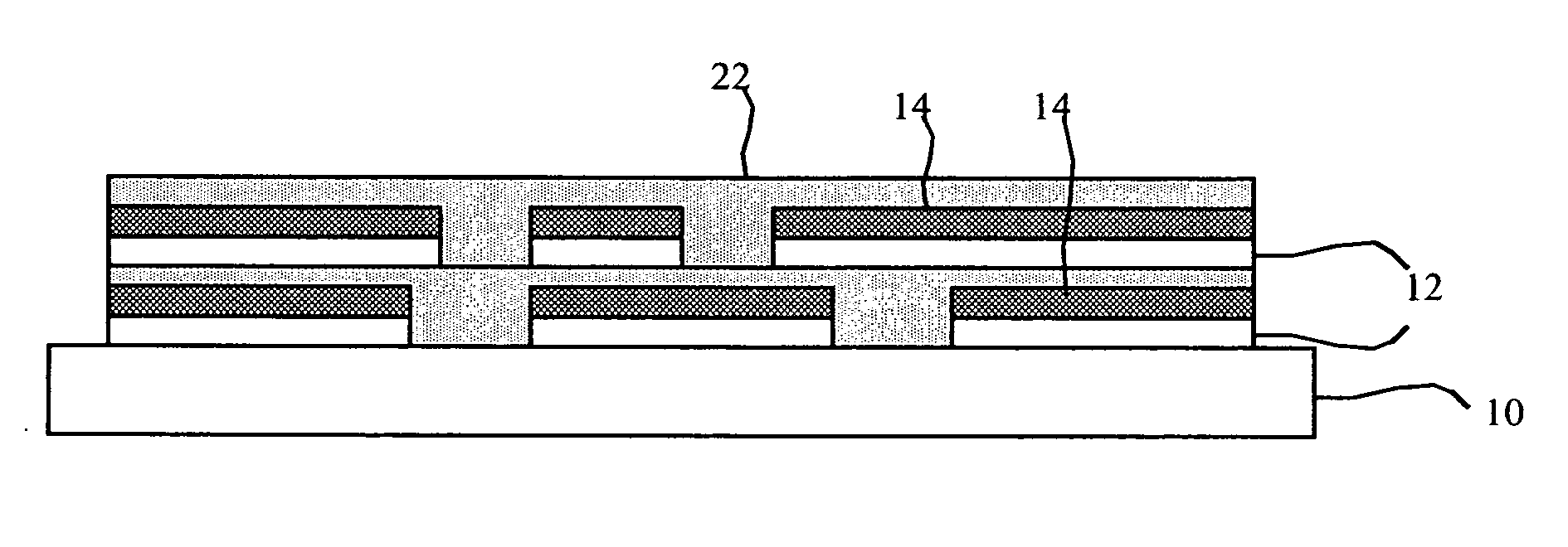
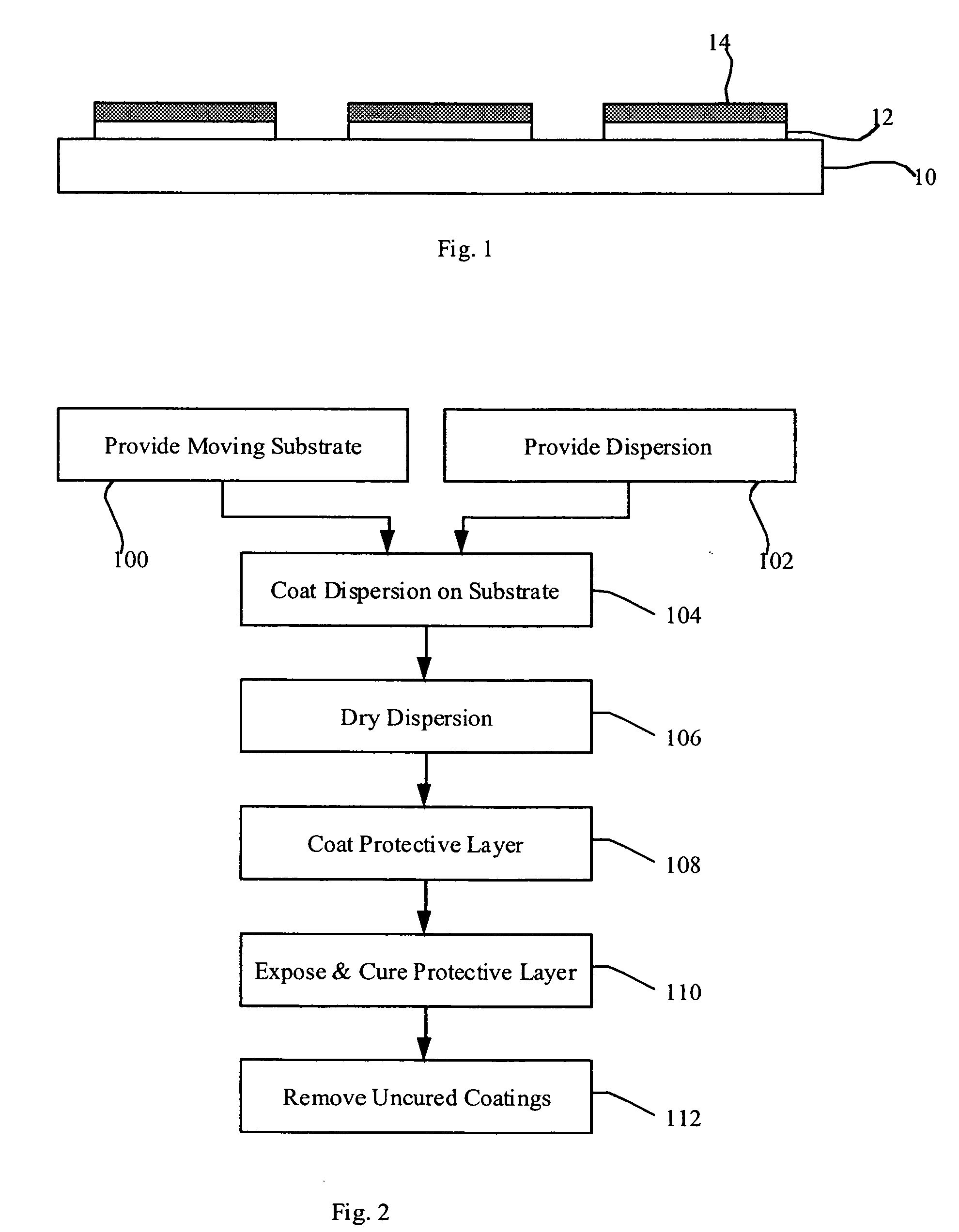
[0016] Referring to FIG. 1, the present invention is directed to a method for manufacturing a patterned conductive coating 12 formed on a substrate 10. The patterned conductor includes a layer of nano-materials, for example, carbon nano-tube conductors or nano-wires, covered by a patterned polymeric resin binder protective layer 14 to hold the nano-materials in place and to protect them from physical trauma. The polymeric resin binder is cured through exposure to radiation and may be transparent or colored using pigments or dyes to provide light absorbing properties. The colors can be, for example, red, green, blue, cyan, magenta, yellow or black. Carbon black may be used to provide a black colorant that will absorb all colors of light.

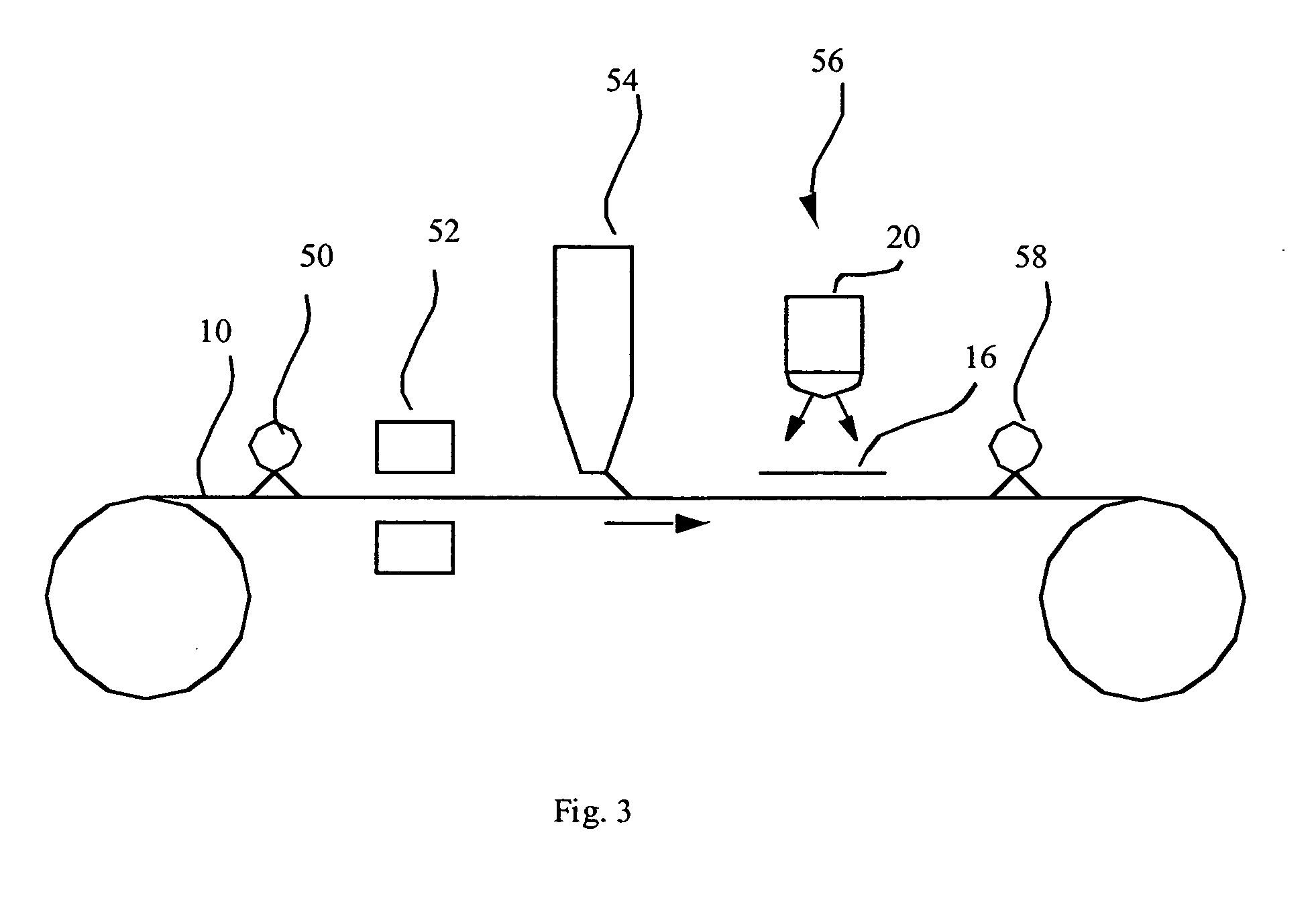
[0017] Referring to FIG. 2, the method of the present invention for continuously manufacturing a patterned conductive layer comprises the steps of providing 100 a linearly moving substrate; providing 102 a dispersion containing conductive nano-materi...


PUM


Abstract

A method of continuously manufacturing a patterned conductive layer includes the steps of providing a linearly moving substrate; coating a dispersion containing conductive nano-materials onto a surface of the linearly moving substrate; drying the coated dispersion wherein the nano-materials self-align into a conductive layer; coating a protective layer of radiation-curable material over the nano-materials coated on the linearly moving substrate; exposing the protective layer coating to patterned radiation and curing the exposed pattern in the protective layer; and removing uncured sections of the protective layer and the underlying sections of the conductive layer to form a patterned conductive layer.

Description

FIELD OF THE INVENTION [0001] The present invention relates to a method for manufacturing patterned conductive coatings and more particularly to the use of nano-materials in such coatings. BACKGROUND OF THE INVENTION [0002] Flat-panel displays rely upon patterned transparent conductive materials deposited on a substrate to provide power to the light emitting or light controlling elements that provide a pixilated display. Such coatings are conventionally made of indium tin oxide (ITO) and are patterned using conventional photolithographic techniques including the deposition of photo-resist, exposing the photo-resist to radiation through a mask, and washing the resulting patterned coating. The coatings of ITO are typically deposited by sputtering at a high temperature. However, such processes are slow and expensive and are not readily employed in continuous manufacturing processes. [0003] Alternative means for providing transparent conductive coatings are known. For example, tiny part...

Claims


Application Information

Patent Timeline
IPC IPC(8): G03F7/00G03F7/11G03F7/20H05K1/09H05K3/00H05K3/06H05K3/28
CPCG03F7/0007G03F7/0035G03F7/11G03F7/2035H05K1/097H05K2203/1545H05K3/06H05K3/064H05K3/28H05K2203/0571H05K3/0023
Inventor COK, RONALD S.
Owner EASTMAN KODAK CO
Why Eureka
Try Eureka