Methods for thermally treating a semiconductor layer

a technology of thermal treatment and semiconductor layer, which is applied in the direction of duplicating/marking methods, sustainable manufacturing/processing, climate sustainability, etc., can solve the problems of high cost and complexity of the transfer layer treatment step, loss of time, and inability to use suitable equipment, so as to improve the crystalline quality and surface roughness of the transfer layer, improve the crystalline quality and the effect of surface roughness

Active Publication Date: 2005-09-08
SOITEC SA
View PDF44 Cites 13 Cited by
  • Summary
  • Abstract
  • Description
  • Claims
  • Application Information

AI Technical Summary

Benefits of technology

[0009] The invention overcomes these problems by presenting methods for forming a semiconductor structure that includes a transfer layer having a good crystalline quality and an improved surface roughness characteristic. An embodiment of the technique includes implanting atomic species into a first surface of a donor wafer to form a zone of weakness at a predetermined depth that defines the thickness of a transfer layer, bonding the first surface of the donor wafer to a host wafer, supplying energy to detach the transfer layer from the donor wafer at the zone of weakness, and conducting a recovery operation on the transfer layer. The recovery operation is conducted after detachment but while the layer remains in contact with the donor wafer. The recovery operation includes heat treating the transfer layer for a predetermined duration at a recovery temperature that is lower than a re-adhesion temperature at which the transfer layer would re-adhere to the donor wafer, to improve the crystalline quality and the surface roughness of the transfer layer.
[0014] The invention advantageously reduces the duration, economic cost and number of treatment devices required for transferring a layer using the SMART-CUT® process. In addition, the method provides a simple way to treat a transfer layer that is easy to incorporate into the SMART-CUT® process, and provides a way to use a recovery heat treatment for the transfer layer both in inert atmosphere and in oxidizing atmosphere without substantially altering the properties of the transfer layer. Further, the method according to the invention improves the crystalline quality of the transfer layer, and makes it possible to produce semiconductor on insulator structures with high crystalline quality and a working layer thickness that can be very thin. The method also reduces the quantity of material removed during treatment of the transfer layer using the SMART-CUT® process. Lastly, the method according to the invention makes it possible to utilize SiGe or Ge for fabricating a semiconductor on insulator structure.

Problems solved by technology

Such a treatment step for the transferred layer 1 is costly and complex.
This results in a loss of time, extra wafer handling and the need to use suitable equipment.
However, selective etching is imprecise, and thus a roughness remains at the tip or edge of the first chemical etching step which is at the interface between the defective zone 1A and the stop layer.
However, the combination of polishing and selective etching further adds to the complexity and cost of the operation, which could make the overall operation unprofitable.
A similar problem exists here analogous to that discussed above, wherein the surface of sound zone 1B is unequally etched because the tip of the etching portion reached it.

Method used


Image

  • Methods for thermally treating a semiconductor layer
  • Methods for thermally treating a semiconductor layer
  • Methods for thermally treating a semiconductor layer

Examples


Embodiment Construction

[0021] Presented below are examples of methods according to the invention, as well as applications, based on transfer layers obtained by using the SMART-CUT® process with Type IV materials or alloys, and in particular with Si1-xGex where x≠0.

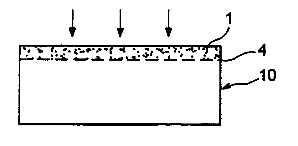
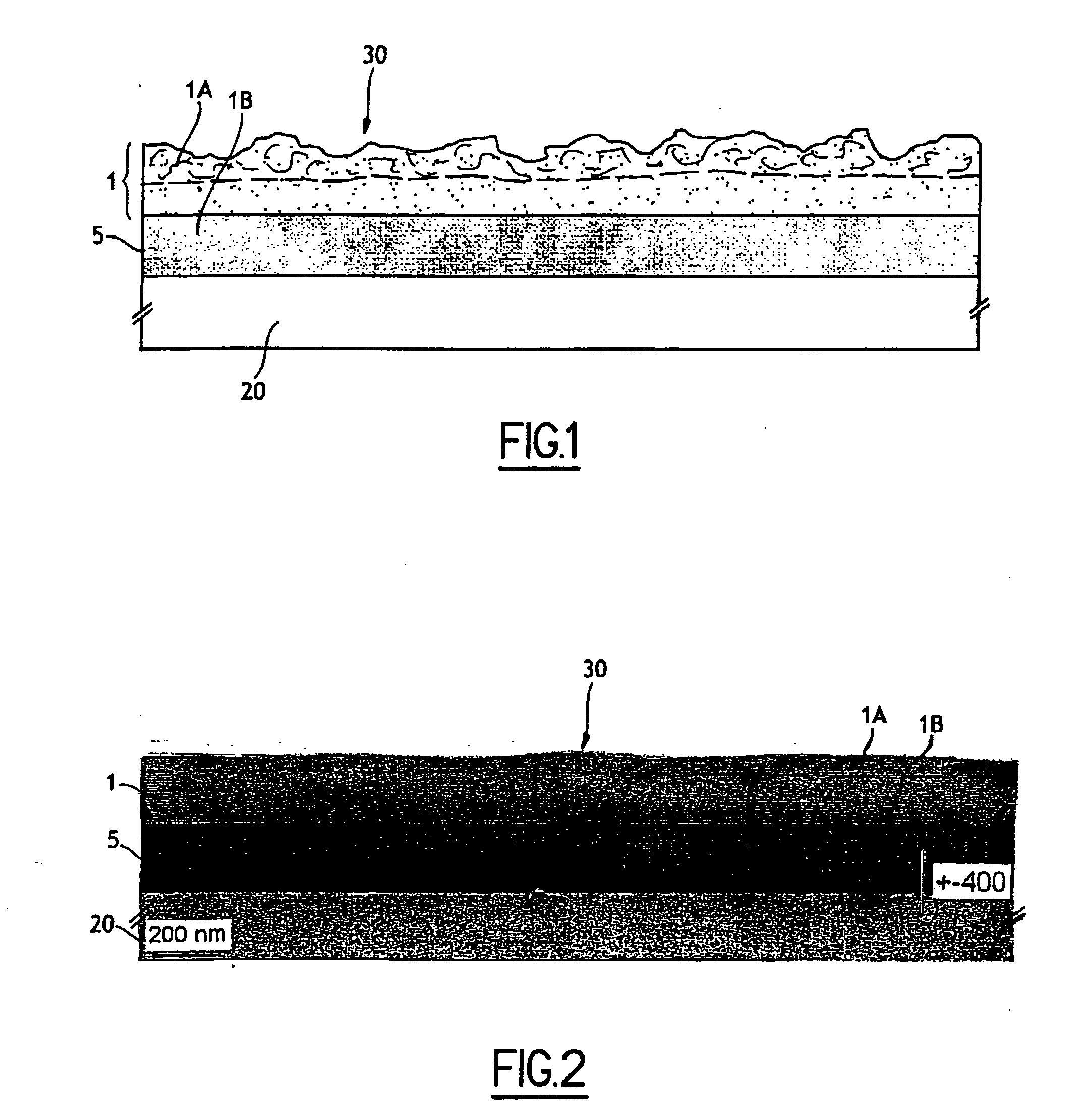
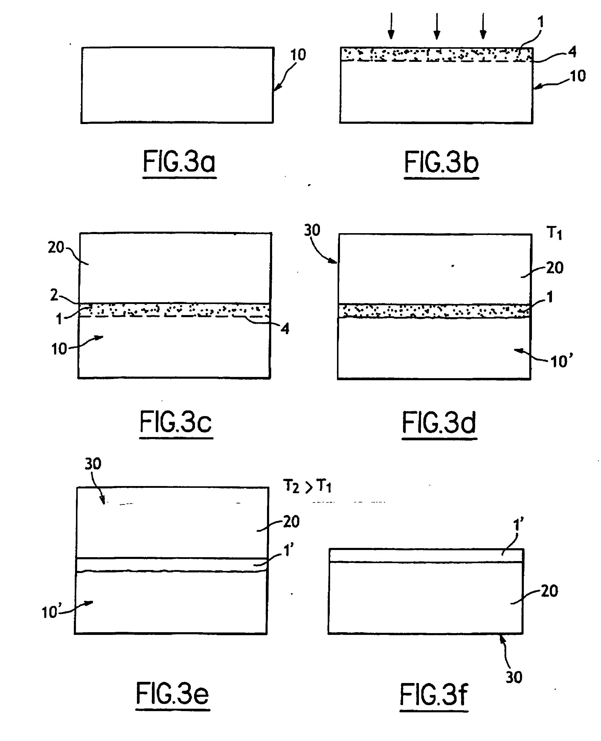
[0022] Referring to FIGS. 3a to 3f, a first method is depicted for transferring a layer of Si1-xGex where x≠0 from a donor wafer to a host wafer. In FIG. 3a, a donor wafer 10 includes a Si1-xGex layer that is to be transferred. Classically, a donor wafer 10 including Si1-xGex comprises a solid Si substrate upon which a buffer structure of SiGe (not shown) has been formed that is made of different layers. The SiGe buffer structure is fabricated to have a gradually increasing amount of Ge through its thickness, starting from 0% at the solid Si substrate level to about 100% at the level of the interface with the upper layer made of Si1-xGex. Of course, the donor wafer 10 may have any other configuration for which a layer of Si1-xGex that is either...


PUM

PropertyMeasurementUnit
temperatureaaaaaaaaaa
recovery temperatureaaaaaaaaaa

Abstract

A method for thermally treating a semiconductor layer is described. An embodiment of the technique includes implanting atomic species into a first surface of a donor wafer to form a zone of weakness at a predetermined depth that defines the thickness of a transfer layer, bonding the first surface of the donor wafer to a host wafer, supplying energy to detach the transfer layer from the donor wafer at the zone of weakness, and conducting a recovery operation on the transfer layer. The recovery operation is conducted after detachment but while the layer remains in contact with the donor wafer. The recovery operation includes heat treating the transfer layer for a predetermined duration at a recovery temperature that is lower than a re-adhesion temperature at which the transfer layer would re-adhere to the donor wafer, to improve the crystalline quality and the surface roughness of the transfer layer.

Description

FIELD OF THE INVENTION [0001] The invention relates to methods for forming a semiconductor structure that includes a transfer layer taken from a donor wafer. The techniques include implanting atomic species to form a zone of weakness zone in the donor wafer that defines a transfer layer, bonding the donor wafer to a host wafer, supplying energy to detach the transfer layer from the donor wafer at the zone of weakness zone, and treating the transfer layer. BACKGROUND ART [0002] A semiconductor layer transfer method called SMART-CUT® is known to those skilled in the art. Details of this method may be found in many published documents, for example, on pages 50 and 51 of: “Silicon on Insulator Technology: Material to VLSI, Second Edition”,” by Jean-Pierre Colinge, published by “Kluwer Academic Publishers”. A second step of bonding the host wafer (the recipient of the transfer layer) typically takes place on the surface of the donor wafer and includes using a bonding layer made of dielec...

Claims


Application Information

Patent Timeline
Patent Type & Authority Applications(United States)
IPC IPC(8): H01L21/762
CPCH01L21/76254Y02P70/50H01L21/30
Inventor DAVAL, NICOLASAKATSU, TAKESHINGUYEN, NGUYET-PHUONG
Owner SOITEC SA
Why Eureka
Try Eureka