Laser based splitting method, object to be split, and semiconductor element chip

a technology of laser based splitting and object, applied in the direction of manufacturing tools, semiconductor/solid-state device details, welding/soldering/cutting articles, etc., can solve the problems of affecting the efficiency of cutting, so as to improve the efficiency, safety, reliability

Active Publication Date: 2005-09-15
CANON KK
View PDF4 Cites 98 Cited by
  • Summary
  • Abstract
  • Description
  • Claims
  • Application Information

AI Technical Summary

Benefits of technology

[0013] The primary object of the present invention is to provide a laser based splitting method capable of ensuring that the cracks which will develop from the internal portion of an object to be split, which has been processed by making a beam of laser light converge to a given point of the internal portion of the object, will be accurately guided to the intended splitting line on the surface of the object, in order to drastically improve the levels of efficiency, safety, and reliability, with which the object is split, and also, to provide an object to be split, and semiconductor chips, which are preferable for accomplishing the above described object of the present invention.

Problems solved by technology

Jetting a stream of water at the cutting point, however, has the following problem: The minute particles of the workpiece itself and the abrasives, which result from the cutting, mix into the cooling water, and are scattered across the wide area including the surfaces which have just been created by the cutting.
This method, however, melts the adjacencies of the point at which the substrate is cut, along with the targeted point; in other words, the adjacencies of the cutting line are damaged.
In particular, when an object to be cut is a piece of semiconductor substrate, there is the problem that the semiconductor circuits on the substrate are damaged across the areas near the cutting lines.
Therefore, the products which result as the melted substances (substrate, etc.) re-solidify adhere to the surface of the substrate, adversely affecting the normal operations of the semiconductor circuits such as logic circuits.
According to the method disclosed in this publication, however, the point where the cutting starts is limited to the area of the substrate where the substrate properties are modified.
Therefore, it is difficult to control the direction and location in which a crack develops toward the substrate surfaces from the point at which the cutting begins, and therefore, it is difficult to cause a crack to develop only in the proper direction and position.
Therefore, if the laser based cutting method disclosed in the abovementioned publication is used to split such an object as the silicon substrate having a minute deviation between the intended splitting line and the crystal orientation of the substrate at the substrate surface, due to the manufacturing errors or the like, which occur during the formation of the silicon substrate and the elements thereon, the crack will miss the intended splitting line as it develops toward the substrate surface.
Therefore, it is highly possible that the logic circuits or the like of the semiconductor elements on the substrate will be destroyed.
Moreover, if unwanted cracks happen to occur, it is impossible to artificially prevent the cracks from growing, and therefore, the circuits on the top surface of the substrate 101 are sometimes damaged.
Therefore, there is the possibility that unwanted cracks will develop from the processed portion 102, progress to the above mentioned internal tubular structures, and destroy the substrate.
In such a case, the object being processed sometimes moves, making it impossible thereafter to precisely trace the intended splitting line with a beam of laser light.

Method used


Image

  • Laser based splitting method, object to be split, and semiconductor element chip
  • Laser based splitting method, object to be split, and semiconductor element chip
  • Laser based splitting method, object to be split, and semiconductor element chip

Examples


embodiment 1

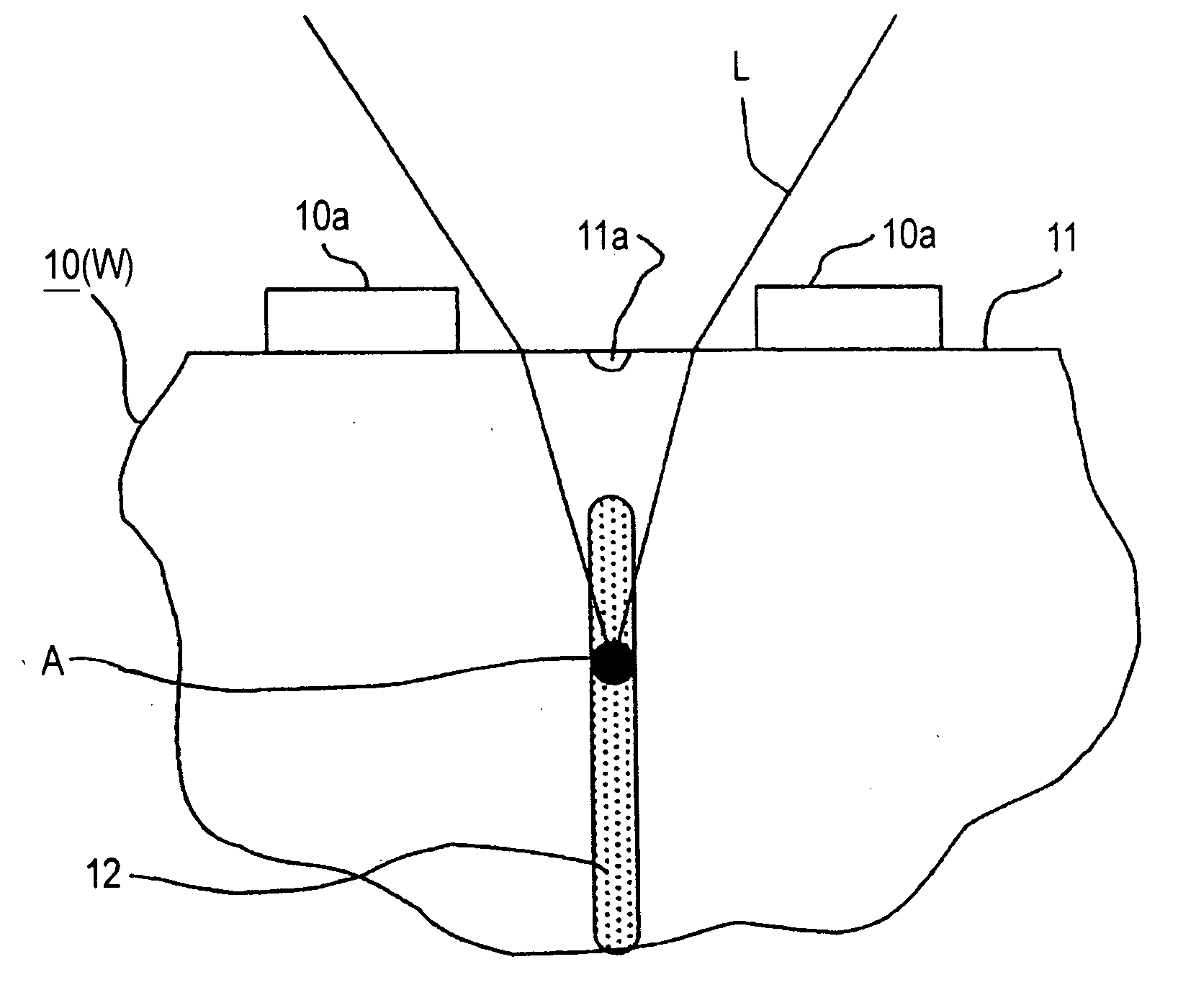
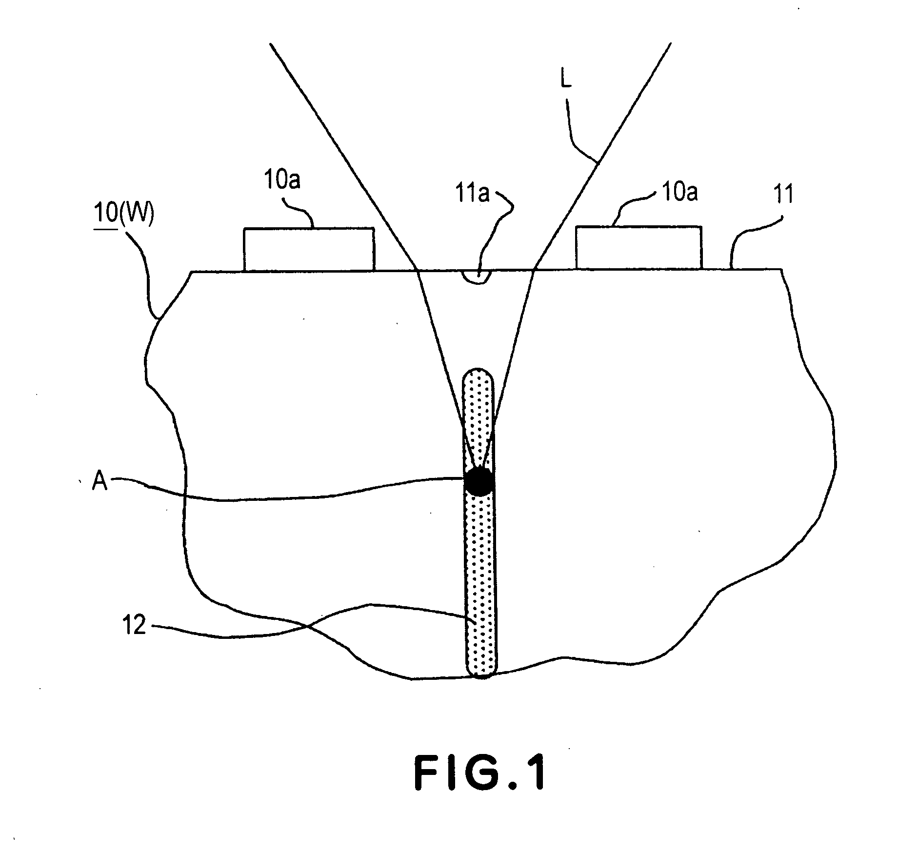
[0066] Next, the method for separating a plurality of element chips, as chips for forming an ink jet head, across each of which the structural components of an ink jet head, such as the circuit, as the logic element 10a, for driving an ink jet head, ink ejection orifices, etc., have been formed, from the silicon substrate 10, will be described.

[0067] The silicon substrate 10 shown in FIGS. 4(a) and 4(b) is formed of a silicon wafer 1 with a thickness of 625 μm, which is formed of a single crystal. Its top surface is parallel to the crystalline orientation (100) of the single crystal. Across the top surface of the silicon wafer 1, an oxide film 2 with a thickness of roughly 1 μm has been formed. On top of the oxide film 2, a plurality of nozzle layers 3 are disposed, which comprises the mechanisms for ejecting liquid such as ink, logic elements for driving these mechanisms, wiring, etc., making up a plurality of logic elements 10a, as shown in FIG. 4(c). Immediately below each nozzl...

embodiment 2

[0166] In the case of the silicon substrate 10, the surface layer of which is a film 2 of silicon dioxide, which is different from the primary substrate material, in order to ensure that the internal cracks are reliably formed, the amount by which a beam of laser light is reflected by the surface of the silicon substrate 10 must be minimized, because the primary cause of the energy loss is that the beam of laser light L is reflected by the surface of the silicon substrate 10.

[0167] Therefore, the silicon substrate splitting process in the first embodiment is partially modified.

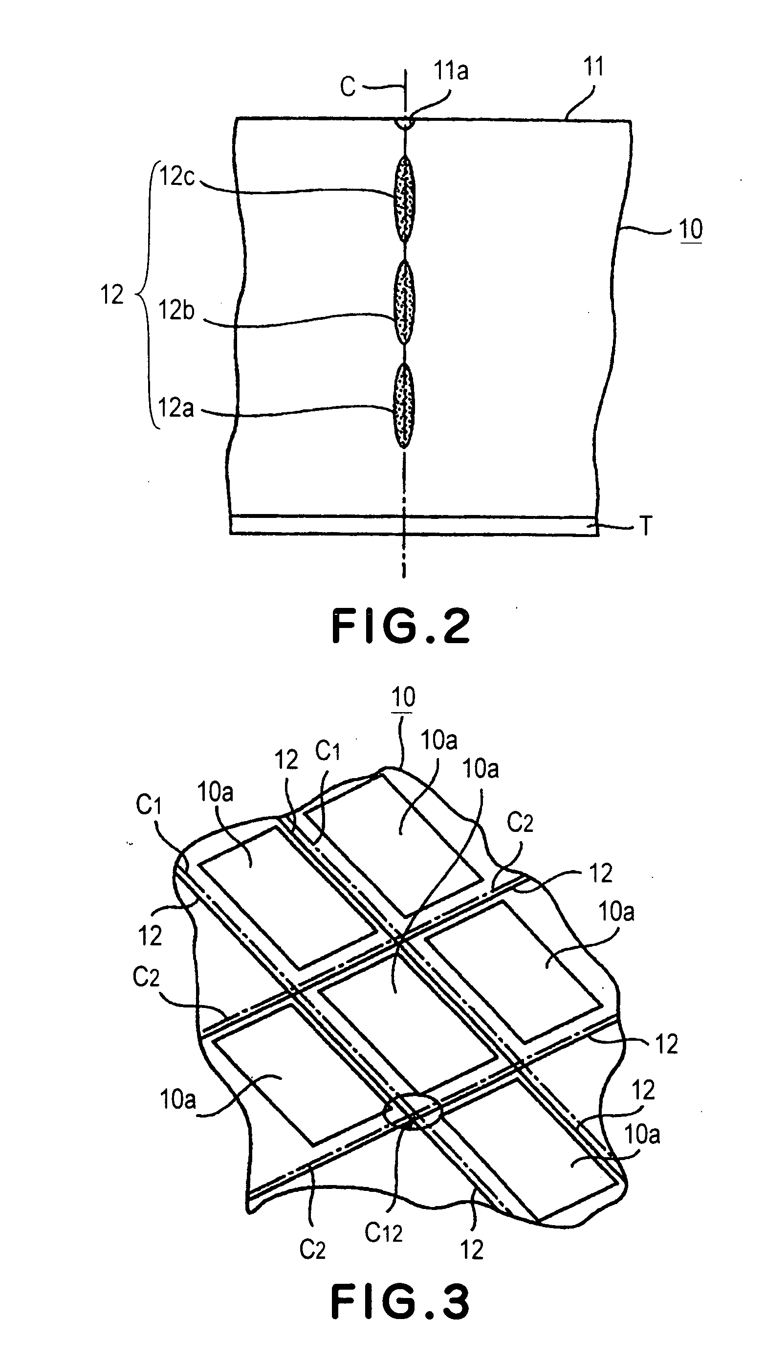
[0168]FIG. 29 is a flowchart of the silicon substrate splitting process in this embodiment. The silicon substrate splitting process in this embodiment comprises: Step 1 for mounting the silicon wafer 1 with the use of adhesive tape; Step 2 for correcting silicon wafer 1; Step 3 for forming a light projection window; Step 4 for forming internal cracks; Step 5 for forming superficial grooves; Step6 for splitti...

embodiment 3

[0174] Referring to FIG. 32(a), the silicon substrate 20 in this embodiment has a plurality of logic elements 20a of an unusual shape, that is, logic elements unusually greater in the ratio between its long and short edges. When splitting this silicon substrate 20 by forming a plurality of internal cracks in the silicon substrate 20, and superficial scratch 21a in the top surface 21 of the silicon substrate 20, the frequency with which the logic elements 20a are damaged while splitting the silicon substrate 20 following the intended splitting line C1, which is parallel to the longer edges of the logic element 20a, is likely to be greater than the frequency with which the logic elements 20a are damaged while splitting the silicon substrate 20 following the intended splitting line C2.

[0175] In particular, if the silicon substrate 20 is such a silicon substrate that holds a plurality of logic elements 20a, each of which is covered with an orifice plate having a liquid ejection orifice...


PUM

PropertyMeasurementUnit
thicknessaaaaaaaaaa
thicknessaaaaaaaaaa
sizeaaaaaaaaaa

Abstract

A laser splitting method for splitting off a segment from an object to be split using a laser beam, includes a surface processing step of processing the object by forming a linear recessed portion in a surface of the object, the linear recessed portion being effective to cause a stress concentration at the surface of the object; an internal processed-region forming step of forming an internal processed-regions at a depth of the object in a line along which a laser beam scans the surface of the object by a relative motion therebetween, the laser beam being converged adjacent the depth, wherein the thus formed internal processed-regions extend in a direction substantially perpendicular to the surface of the object; and an external force applying step of applying an external force to the object to form cracks between the recessed portion and the internal processed-regions.

Description

FIELD OF THE INVENTION AND RELATED ART [0001] The present invention relates to a method for splitting an object by causing a beam of laser light to converge on the object to be split. It also relates to an object across which a plurality of semiconductor element circuits (a plurality of semiconductor chips) are present, and which is slit with the use of the laser based splitting method, and the semiconductor element chips. [0002] As for the method, in accordance with the prior art, for splitting an object, the blade dicing method has been known, according to which a blade in the form of a disc, the thickness of which is in the range of several tens of micrometers—hundreds of micrometers is rotated at a high speed, and a piece of semiconductor substrate (which hereinafter may be referred to as workpiece) is separated into a plurality of pieces as the substrate is cut by the abrasive substances on the surface of the blade. In the case of this method, it has been a common practice to j...

Claims


Application Information

Patent Timeline
Patent Type & Authority Applications(United States)
IPC IPC(8): B28D5/00B23K26/38B23K26/40B23K101/40H01L21/301
CPCB23K26/0057B23K26/4075B28D5/0011B23K26/0676H01L21/78B23K26/0617H01L21/67092B23K26/40B23K26/53B23K2103/50B23K26/082
Inventor IRI, JUNICHIROINADA, GENJISUGAMA, SADAYUKINISHIWAKI, MASAYUKIMORIMOTO, HIROYUKI
Owner CANON KK
Why Eureka
Try Eureka