
Detection of defects in patterned substrates

a technology of patterned substrates and defects, applied in the direction of individual semiconductor device testing, semiconductor/solid-state device testing/measurement, instruments, etc., can solve the problems of optical undetectable defects, more than 50% of killer defects arising in processes using 0.35 .mu.m design rules, and optical undetectable defects

Inactive Publication Date: 2005-09-15
APPLIED MATERIALS INC
View PDF2 Cites 37 Cited by
  • Summary
  • Abstract
  • Description
  • Claims
  • Application Information

AI Technical Summary

Benefits of technology

The system significantly reduces stage-move overhead, enabling faster defect detection across semiconductor wafers with improved resolution and coverage, effectively identifying both surface and sub-surface defects without compromising throughput.

Problems solved by technology

Optical tools are inherently limited by diffraction and depth of focus.
As a result, more than 50% of killer defects arising in processes using <0.35 .mu.m design rules prove to be optically undetectable defects.
Killer defects are defects which adversely affect electrical performance of a device at final test of the device.
Trends indicate that this problem will become worse, especially for metal interconnect layers with sub-surface defects.
This is due to the small depth of focus of conventional optical inspection tools, an inherent limitation of the large numerical aperture objective lenses required to image sub-micron features.
Thus any defect that is not at the device surface will be substantially out of focus and therefore undetectable.
All of these result in either an electrical “open” or “short” type defect.
Also, diffraction-limited resolution renders small surface defects undetectable as minimum critical dimensions (CDs) shrink below 0.25 .mu.m.
Conventional SEMs are too slow, however, to cover a statistically significant wafer area or number of defects in a short enough period of time.
This limitation stems primarily from the slow serial nature of the data-collection process, though also in part from a general lack of automation.
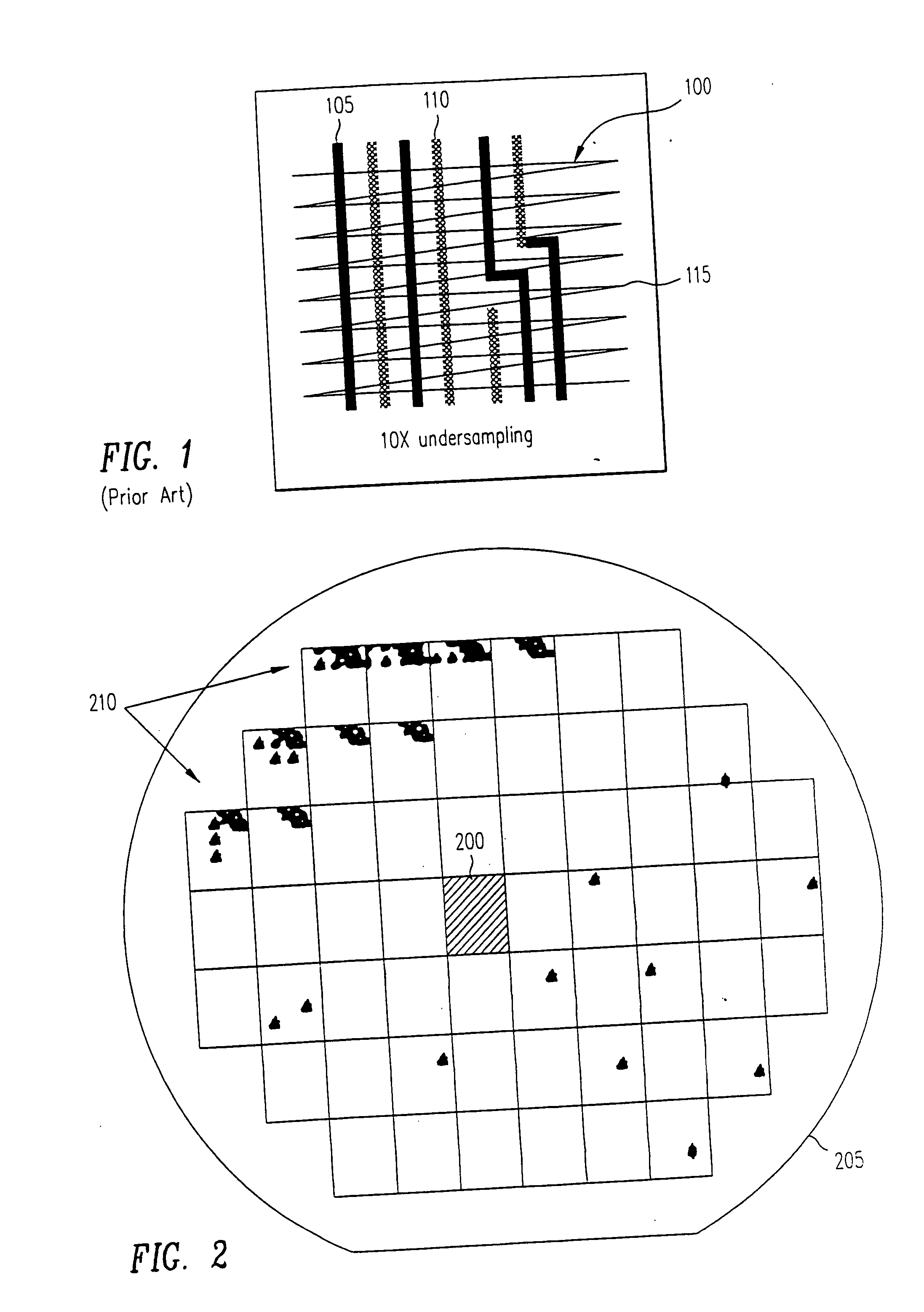
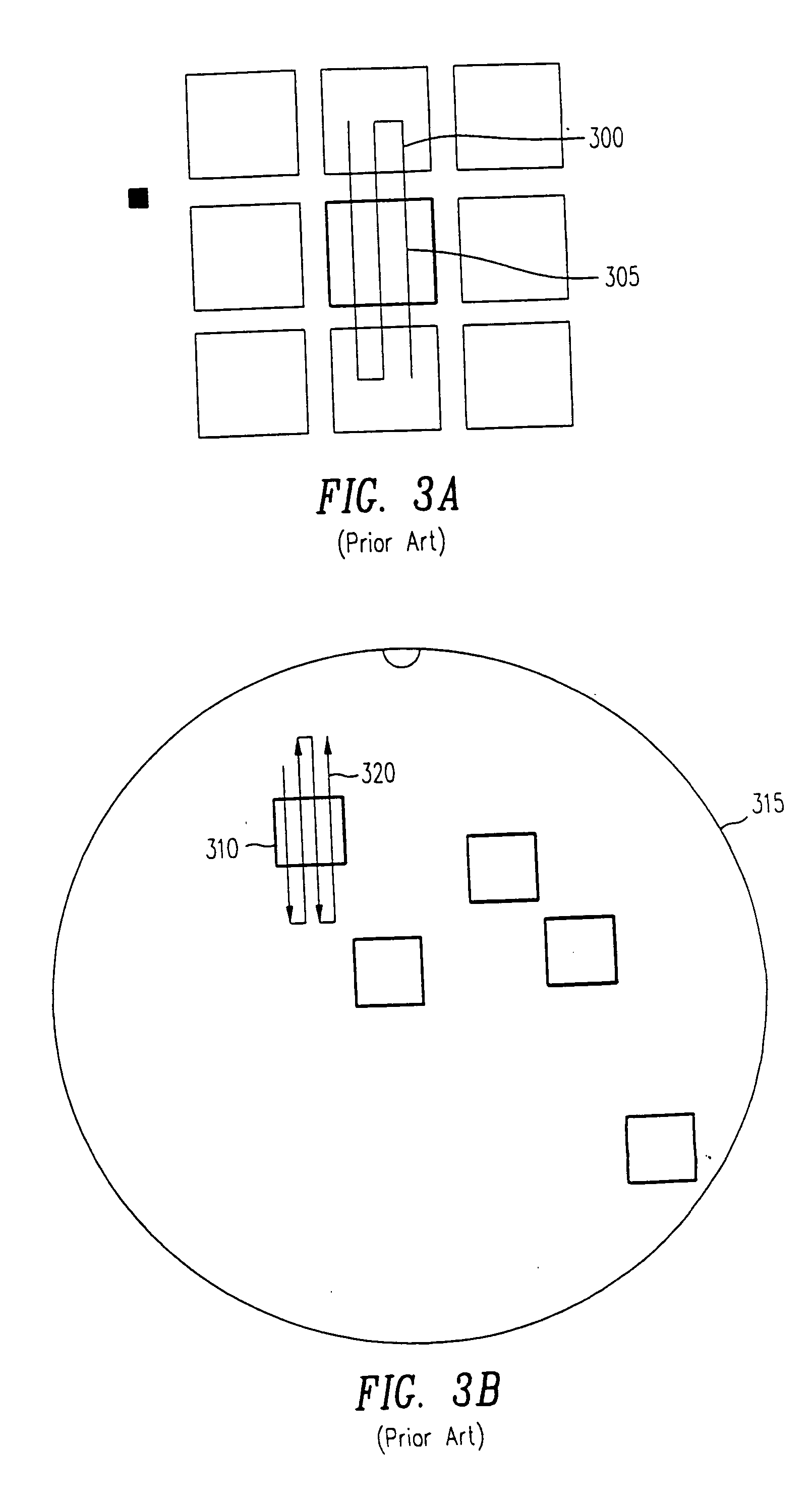
In addition the time taken to move the mechanical stage to each new imaging position is large compared to the imaging time and thus limits throughput even with automation features.
It is unfortunately not as effective with layers having other characteristics, e.g., layers with small features such as vias, contacts, localized interconnects and memory cells.
This approach is also unlikely to detect small particles or missing or extra patterns.
Presently available systems lack such flexibility.
A challenge with the apparent-feature enlargement approach is that multiple layers of the database and knowledge of the electrical properties of the circuit represented are required to determine which features are grounded and which are floating in negative charge mode, e.g., which p-n junctions are forward biased by the negative potential or voltage.

Method used


Image

  • Detection of defects in patterned substrates
  • Detection of defects in patterned substrates
  • Detection of defects in patterned substrates

Examples


example 1

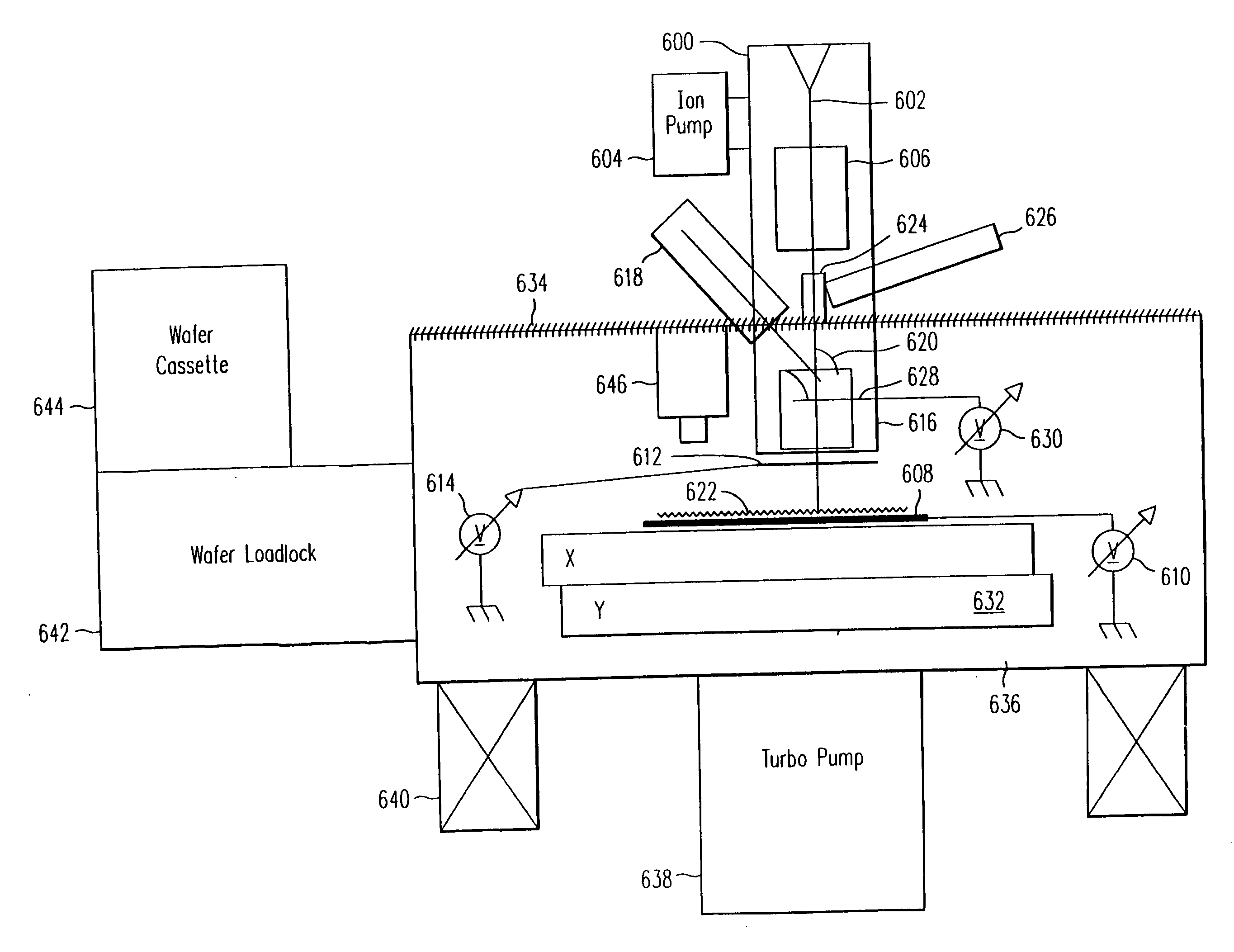
[0043] The following typical parameters are assumed for “Case 1” and “Case 2”:

[0044] die size=1 cm.sup.2

[0045] pixel resolution=25 nm

[0046] pixel rate=100 MHz

[0047] FOV of small-FOV lens 25 .mu.m.times.25 .mu.m (1,000 pixels per line, same as the sub-FOV of large-FOV lens)

[0048] FOV of large-FOV lens=1 mm.times.1 mm

[0049] time for a single stage move=1 second

[0050] time for scanning stage to reverse direction and re-accelerate to constant speed=.about.3 seconds

[0051] Case 1: Time to acquire image of a single die using large FOV lens with step and image mode (consistent with the present invention)

Stage-Move Overhead:100 stage moves = 100 secondsData acquisition time:acquire 16 ×. 1010 pixels =1600 secondsTotal time required:stage moves + acquisition =1700 secondsEfficiency (data1600 / 1700 =94%acquisition time / total time):

[0052] Case 2: Time to acquire image of a single die using small FOV lens with a continuously scanning staging (prior art)

Stage-Move Overhead:time to reve...

example 2

[0053] As indicated in Table 1 below, this example assumes a 1 mm.times. 1 mm FOV for the large-FOV objective lens and a 40 MHz pixel-data acquisition rate. The time for the stage to move and settle is conservatively assumed to be 1 second (typically a well-designed stepping stage would move and settle in <0.5 second). With these assumptions, the stage move overhead represents .about.3% of the total image acquisition time. That is, an ideal stage which would move and settle instantaneously would only result in only a .about.3% through-put increase. Thus the stage-move overhead is of little consequence.

TABLE 1Critical0.18 μmNo pre-chargeDimensions (CD)Pixels / CD4Data rate =4.00E+07 HzPixel size=0.45 μmAvg. =2Pixels / cm=222222Time / sub FOV =0.05 sPixels / cm =49382716049Beam vector time =200 μmTotal Time / sub FOV =0.05 sFOV (per side) =1 mmTinx / FOV =24.8 sFOV / cm2100Pixels / FOV line =22222Stage move / settle time  1 sPixels / sub FOV1000Overhead (focus, etc) =0.15Line =Sub FOV / line =22.2Total t...


PUM

PropertyMeasurementUnit
timeaaaaaaaaaa
timeaaaaaaaaaa
landing energyaaaaaaaaaa

Abstract

One embodiment of the present invention is a method of detecting defects in a patterned substrate, including: (a) positioning a charged-particle-beam optical column relative to a patterned substrate, the charged-particle-beam optical column having a field of view (FOV) with a substantially uniform resolution over the FOV; (b) operating the charged-particle-beam optical column to acquire images of a region of the patterned substrate lying within the FOV by scanning the charged-particle beam over the patterned substrate; and (c) comparing the acquired images to a reference to identify defects in the patterned substrate.

Description

CROSS-REFERENCE TO RELATED APPLICATIONS [0001] This application is a divisional of U.S. patent application Ser. No. 10 / 134,210, filed Apr. 29, 2002, which is a continuation of U.S. patent application Ser. No. 09 / 846,487, filed Apr. 30, 2001, which in turn is a divisional of U.S. patent application Ser. No. 09 / 226,967, filed Jan. 8, 1999, now U.S. Pat. No. 6,252,412, all incorporated by reference in their entireties. [0002] This application is related to U.S. patent application Ser. No. 08 / 892,734 filed Jul. 15, 1997, U.S. patent application Ser. No. 08 / 782,740 filed Jan. 13, 1997, U.S. patent application Ser. No. 09 / 012,227 filed Jan. 23, 1998, U.S. patent application Ser. No. 09 / 226,962 filed on Jan. 8, 1999, and U.S. patent application Ser. No. 09 / 227,747 filed on Jan. 8, 1999, and U.S. patent application Ser. No. 09 / 227,395 filed on Jan. 8, 1999, all incorporated herein by reference in their entireties.TECHNICAL FIELD OF THE INVENTION [0003] One or more embodiments of the present...

Claims


Application Information

Patent Timeline
Patent Type & Authority Applications(United States)
IPC IPC(8): G01R31/302G01B15/00G01N21/00G01N23/00G01N23/04G01N23/225G01Q30/04G01Q40/02G01R1/06G01R31/265G01R31/305H01J37/073H01J37/20H01J37/22H01J37/256H01J37/28H01L21/66
CPCG06T7/0004H01J37/265H01J37/28H01J2237/2817H01J2237/221H01J2237/24592H01J2237/2485H01J2237/202H01L22/00
Inventor TALBOT, CHRISTOPHER G.LO, CHIWOEI WAYNE
Owner APPLIED MATERIALS INC
Learn More