

Semiconductor device and fabrication process thereof
a technology of semiconductor devices and resistance elements, which is applied in the direction of instruments, natural mineral layered products, transportation and packaging, etc., can solve the problems of difficult increase of integration density of integrated circuits, difficult formation of highly miniaturized patterns, and easy oxidation of metal thin-film bodies b>77/b>, etc., to achieve stable resistance value, short time period, and low cost
- Summary
- Abstract
- Description
- Claims
- Application Information
AI Technical Summary
Benefits of technology
Problems solved by technology
Method used
Image

Examples
Embodiment Construction
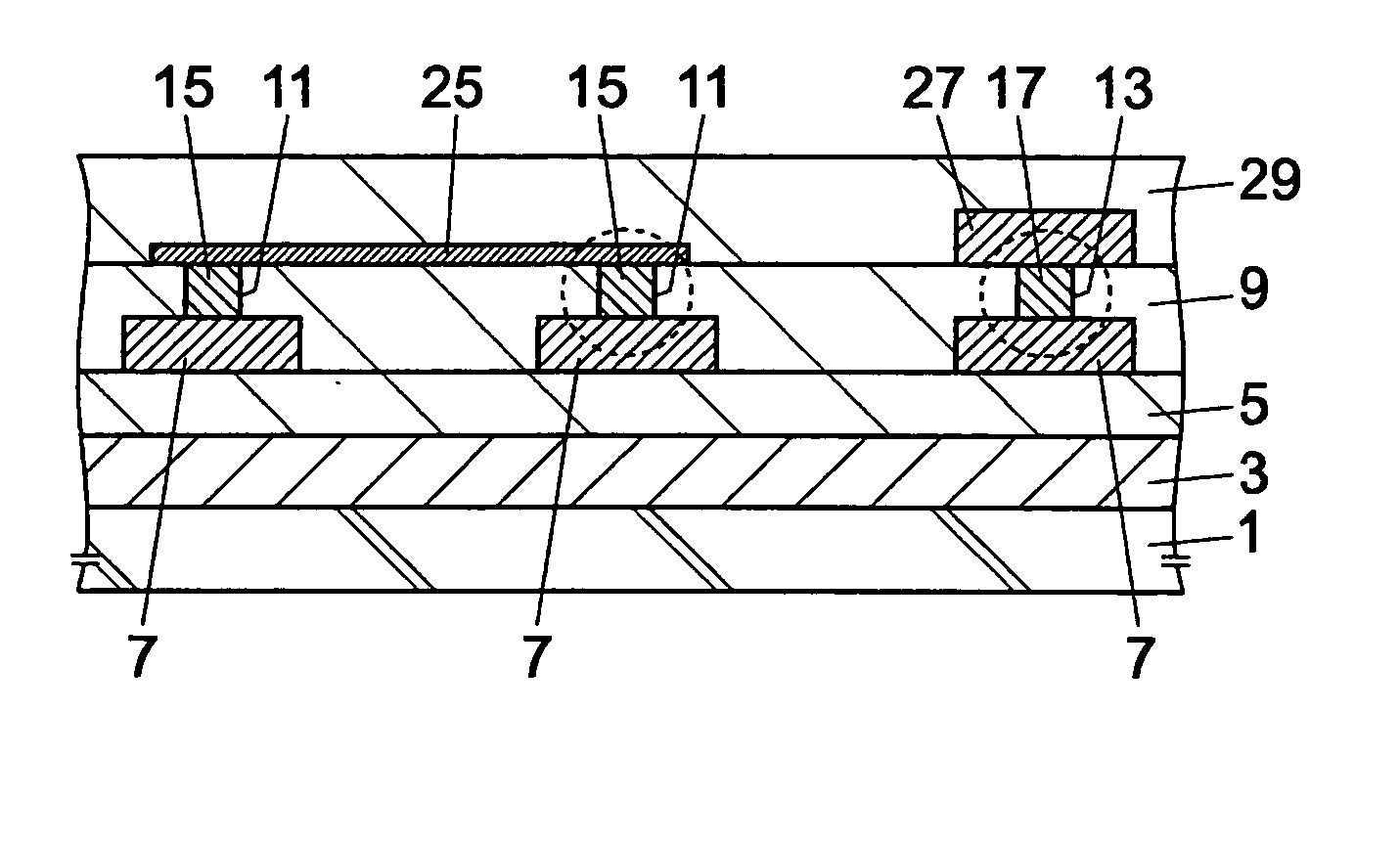
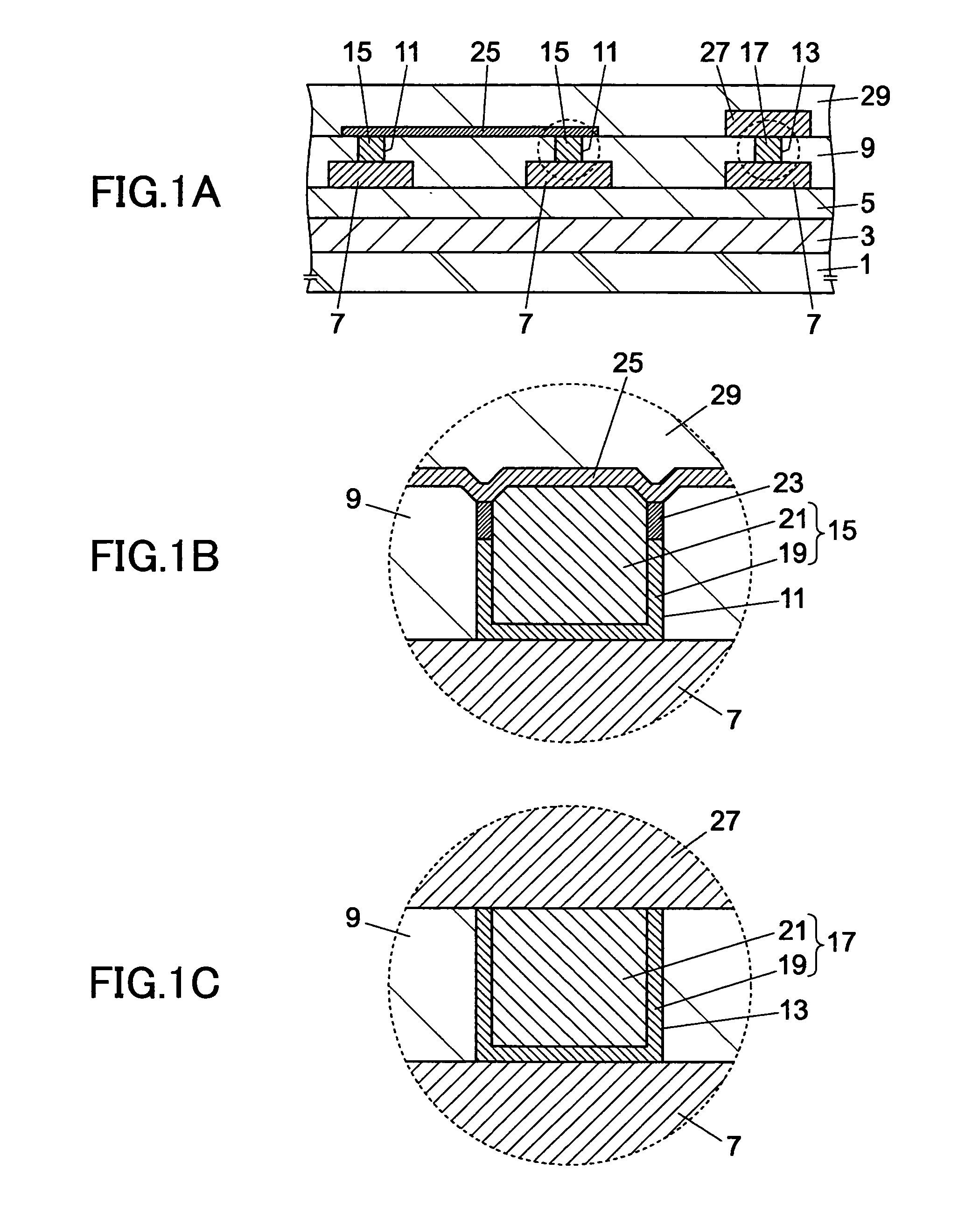
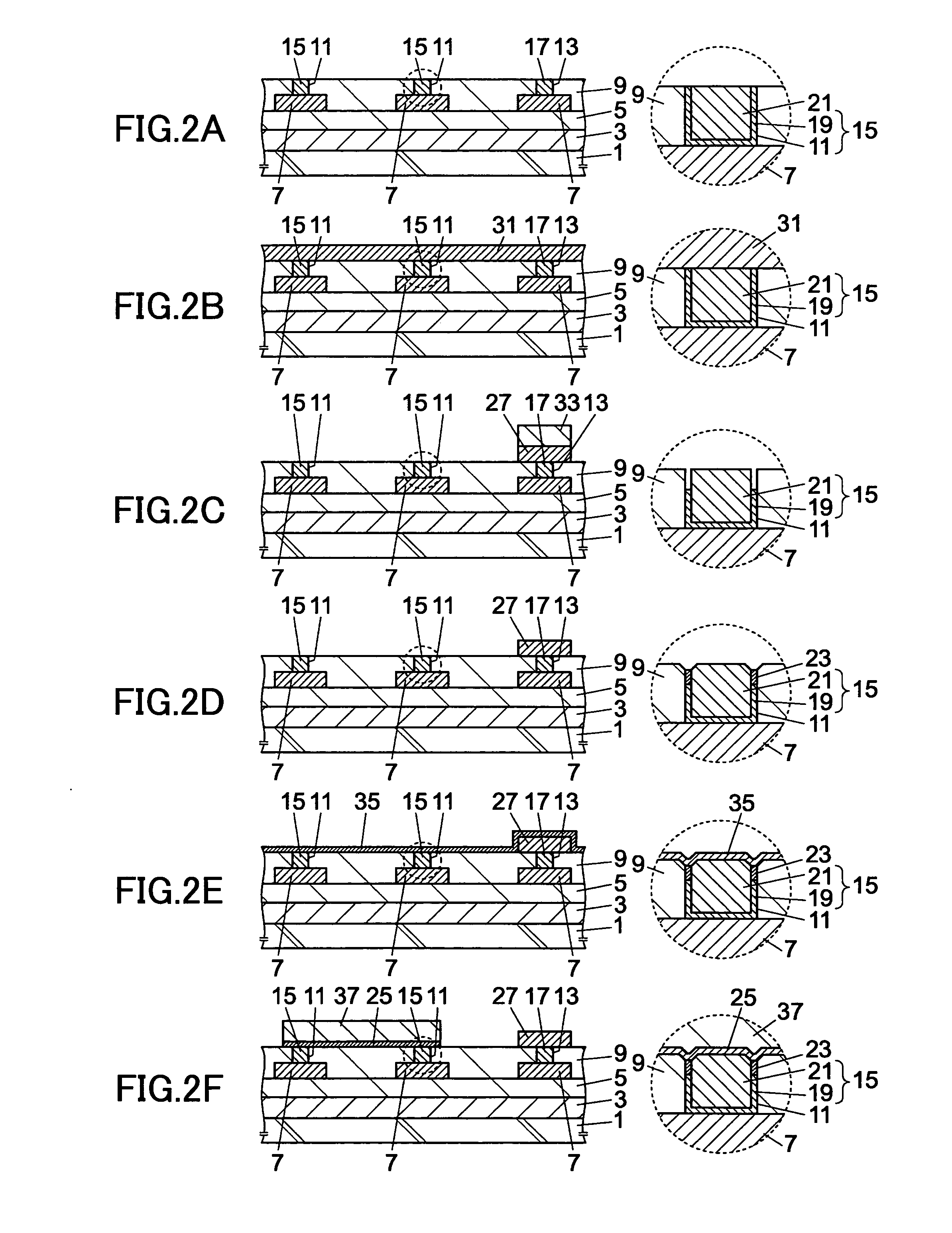
[0155]FIGS. 1A-1C are diagrams showing the semiconductor device according to an embodiment of a first mode of the present invention, wherein FIG. 1A shows the construction of the semiconductor device in a cross-sectional view, FIG. 1B shows a first contact hole thereof with magnification, while FIG. 1C shows a second contact hole thereof with magnification. In the embodiment described hereinafter, it should be noted that there are formed also transistors and capacitors not illustrated on the common substrate.
[0156] Referring to the drawings, there is formed a device isolation oxide film 3 on a silicon substrate 1, wherein the silicon substrate 1 is formed with a first interlayer insulation film 5 of BPSG or PSG (phoshosilicate glass) such that the first interlayer insulation film 5 covers the region where the device isolation oxide film 3 is formed.
[0157] On the first interlayer insulation film 5, there is formed a first-layer metal interconnection pattern 7, wherein the first-lay...
PUM
| Property | Measurement | Unit |
|---|---|---|
| depth | aaaaa | aaaaa |
| thickness | aaaaa | aaaaa |
| thickness | aaaaa | aaaaa |
Abstract
Description
Claims
Application Information