Semiconductor chip capable of implementing wire bonding over active circuits
a technology of active circuits and semiconductors, applied in the field of semiconductor integrated circuits, can solve the problems of limited pad area of chips, impose constraints on wire bonding, and more costly choice to counteract this trend, and achieve the effect of saving valuable silicon area
- Summary
- Abstract
- Description
- Claims
- Application Information
AI Technical Summary
Benefits of technology
Problems solved by technology
Method used
Image

Examples
second embodiment
[0021]FIG. 3 is a schematic cross-sectional diagram illustrating pivotal portions of an exemplary integrated circuit capable of implementing BOAC in accordance with the third preferred embodiment of the present invention, in which like numerals refer to like elements. As shown in FIG. 3, the integrated circuit 1 according to the present invention comprises a bonding pad area 10 and an active circuit area 12. A bonding pad reinforcement structure 300 is disposed within the bonding pad area 10. Portions of the active circuit components 120 of the integrated circuit 1 are situated directly under the bonding pad reinforcement structure 300. The active circuit components 120 may include input / output (I / O) devices / circuits, or Electrostatic Discharge (ESD) devices / circuits, each of which may further consist of a plurality of semiconductor devices, which are fabricated on a main surface of a substrate 200, for example, such as metal-oxide-semiconductor field-effect transistors (MOSFETs), i...
first embodiment
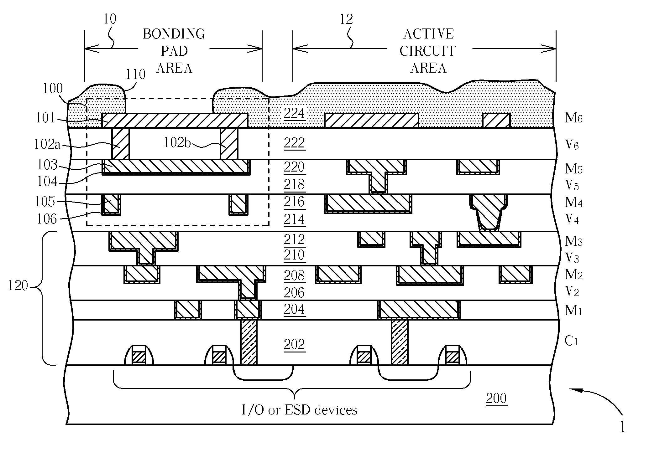
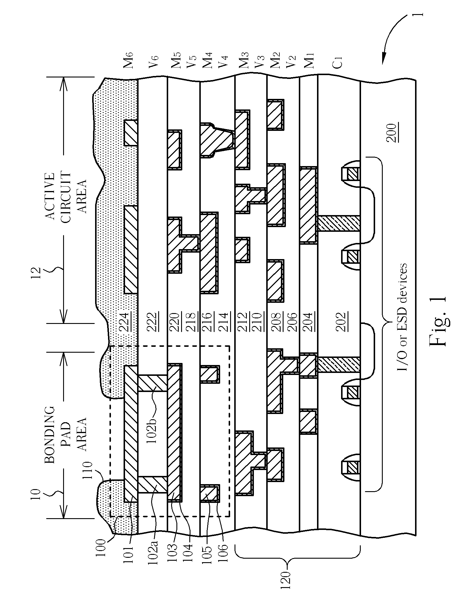
[0024] The metal interconnection M5 is defined in the low-k dielectric layer 220 using damascene method known in the art to form designed circuit layout within the active circuit area 12 and to form a damascened intermediate metal layer 103 within the bonding pad area 10. The damascened intermediate metal layer 103 also acts as a bussing metal layer. Damascene via devices (V5) within the active circuit area 12 for connecting M4 with M5 are fabricated in low-k dielectric layer 218. The metal interconnection M6 is defined on the stress-buffering dielectric layer 222 using conventional aluminum wiring method known in the art to form designed circuit layout within the active circuit area 12 and to form a contact pad 101 having a top surface area adequate for landing balls of bonding wires or solder within the bonding pad area 10. Via devices (V6) within the active circuit area 12 for connecting M5 with M6 are fabricated in the stress-buffering dielectric layer 220. It is one of the pivo...
PUM
| Property | Measurement | Unit |
|---|---|---|
| thickness | aaaaa | aaaaa |
| thickness | aaaaa | aaaaa |
| thickness | aaaaa | aaaaa |
Abstract
Description
Claims
Application Information