

Method of Manufacturing Single-Crystal GaN Substrate, and Single-Crystal GaN Substrate
a technology of crystal gan and single crystal gan, which is applied in the direction of crystal growth process, polycrystalline material growth, chemically reactive gas, etc., can solve the problems of large portion lost to waste, long, and inability to grow single crystal ingots from liquid phase,
- Summary
- Abstract
- Description
- Claims
- Application Information
AI Technical Summary
Benefits of technology
Problems solved by technology
Method used
Image

Examples
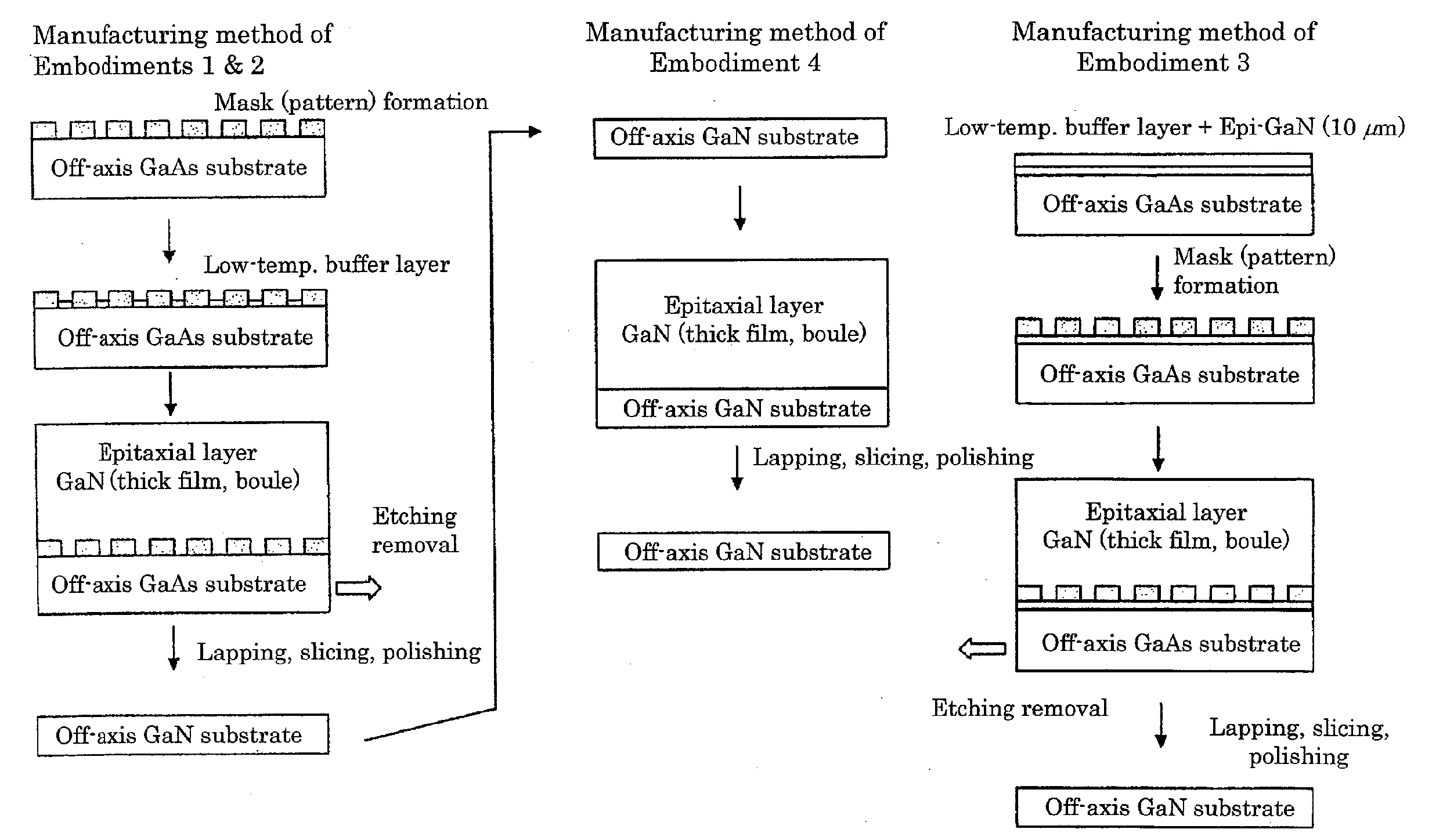
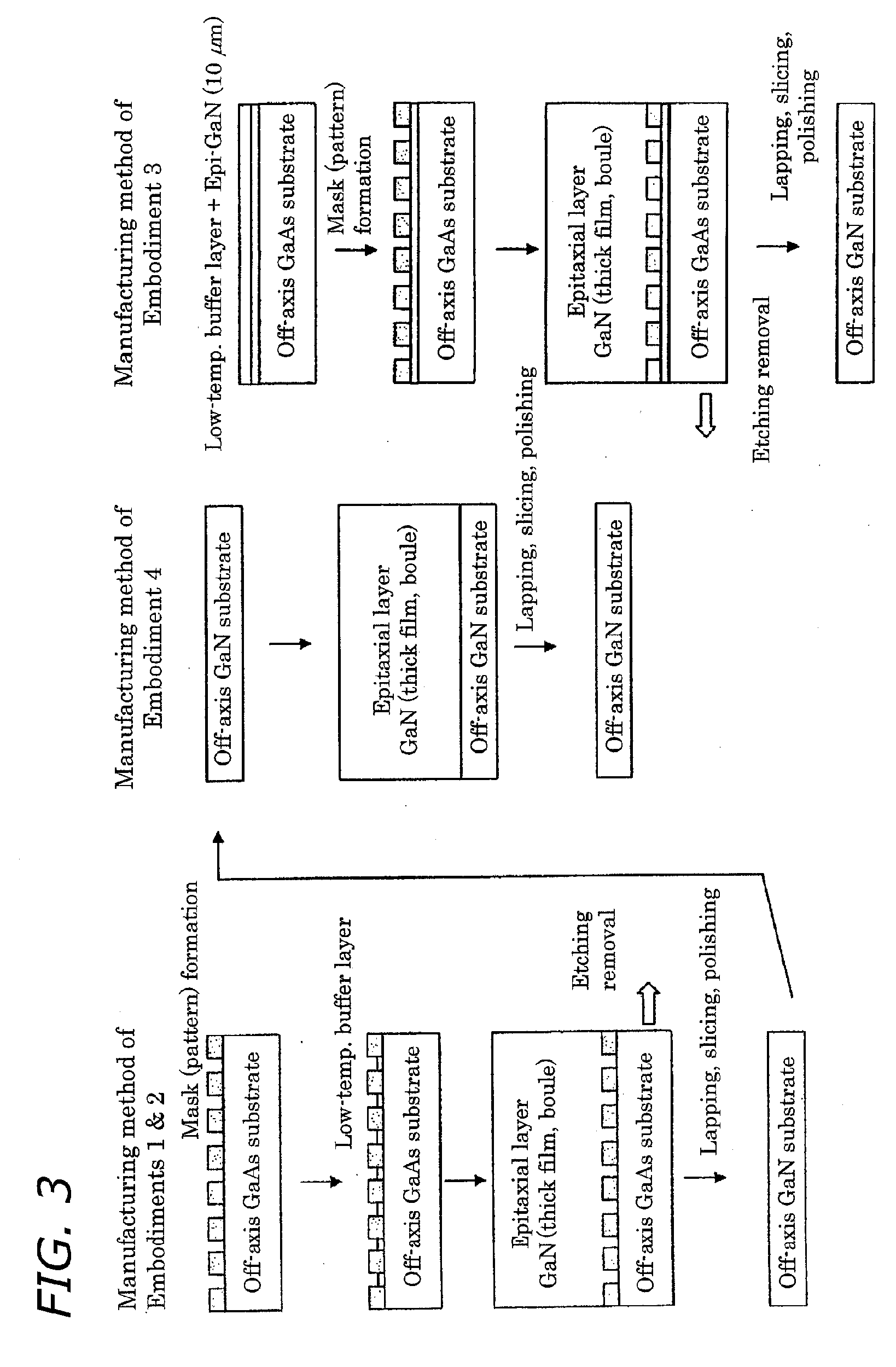
embodiment 1
Method of Manufacturing Off-Axis GaN Substrates by Growing GaN Crystal onto a Misoriented GaAs Substrate on which an ELO Mask is Layered or is not Layered
[0071] By a procedure as follows, GaN crystal was produced atop an off-axis GaAs starting substrate, made into a freestanding film, lapped and polished, and examined as to its misorientation and its crystalline properties.
[0072] The (111) A face of off-axis GaAs was utilized as the starting substrate. GaAs is a cubic-system crystal of the zincblende (ZnS) type. The GaAs (111) planes are faces in which there is threefold rotational symmetry. The GaAs (111) planes comprise a face in which only Ga appears in the surface, and a face in which only As atoms appear in the surface. The former is called the (111) Ga face or the (111) A face; the latter is called the (111) As face or the (111) B face. In the present embodiment, GaAs (111) crystal was used with the Ga face facing up.
[0073] Since a (111) Ga face has threefold symmetry, hex...
embodiment 2
Method of Manufacturing Off-Axis GaN Substrates by Growing GaN Crystal onto a Misoriented GaAs Substrate on Which GaN is Grown Thin, and a Patterned ELO Mask is Provided or is not Provided
[0124] In Embodiment 1, an ELO mask was provided (or not provided) directly onto a miscut GaAs starting substrate, and GaN was epi-grown onto the masked / maskless substrate. In Embodiment 2 what was done was to put a GaN epilayer thinly onto a miscut GaAs substrate, provide (or not provide) an ELO mask on the epilayered substrate, and epi-grow GaN onto the thus prepared substrate. That is, this makes it so that the growth of GaN is in two stages, with ELO growth being done intermediately. Misoriented GaN crystal produced in this way was lapped and polished to yield smooth flat wafers, and the misorientation and crystal properties of the wafers were examined.
[0125] Likewise as in Embodiment 1, miscut GaAs substrates with the Group I misorientations—in which the GaAs [111] direction was inclined 0....
embodiment 3
Method of Manufacturing a Plurality of GaN Wafers by Growing GaN Thick onto a Misoriented GaAs Substrate, and Cutting Through the GaN Crystal
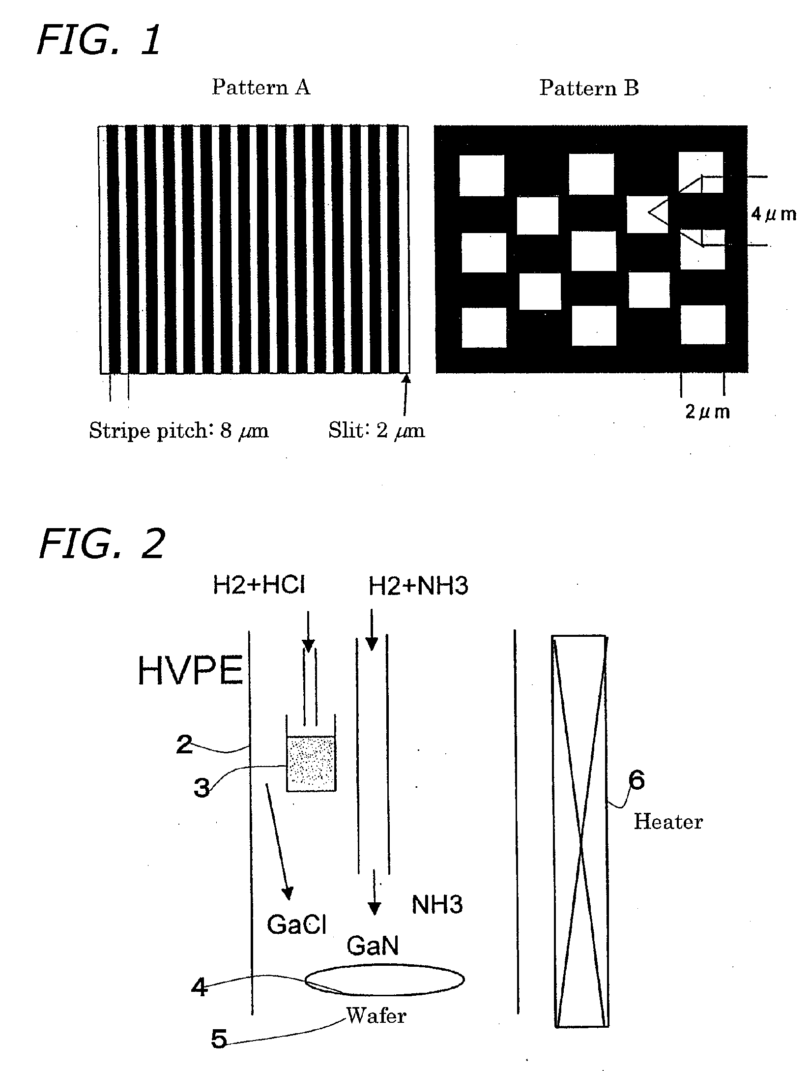
[0159] A plurality of GaN wafers was prepared with, as starting substrates, GaAs substrates inclined in either of two directions and of seven differing misorientations, onto which a Pattern-A ELO mask, a Pattern-B ELO mask, or no mask was formed, by initially growing a thin GaN buffer layer, and afterwards a thick (10 mm) GaN epilayer, and cutting through the GaN parallel to the growth plane. The characteristics of the GaN wafers thus prepared were examined.
GaAs (111) A Face
[0160] Inclination angles: 0.1°, 0.3°, 1°, 5°, 10°, 20° and 25°. [0161] Group I—GaAs [111] direction inclined towards a direction. [0162] Group II—GaAs [111] direction inclined towards a direction. [0163] Type 1—Substrates in which an ELO mask of Pattern A was formed onto a GaN film; [0164] Type 2—Substrates in which an ELO mask of Pattern B was formed onto a GaN film...
PUM
| Property | Measurement | Unit |
|---|---|---|
| thickness | aaaaa | aaaaa |
| off-axis angle | aaaaa | aaaaa |
| off-axis angle | aaaaa | aaaaa |
Abstract
Description
Claims
Application Information