

Trench power MOSFET fabrication using inside/outside spacers
a technology of inside/outside spacers and mosfets, which is applied in the direction of basic electric elements, electrical equipment, semiconductor devices, etc., can solve the problems of difficult to reduce the width of the trench, and inconvenient operation, etc., to achieve the effect of reducing width, high conductivity, and increasing cell density
- Summary
- Abstract
- Description
- Claims
- Application Information
AI Technical Summary
Benefits of technology
Problems solved by technology
Method used
Image

Examples
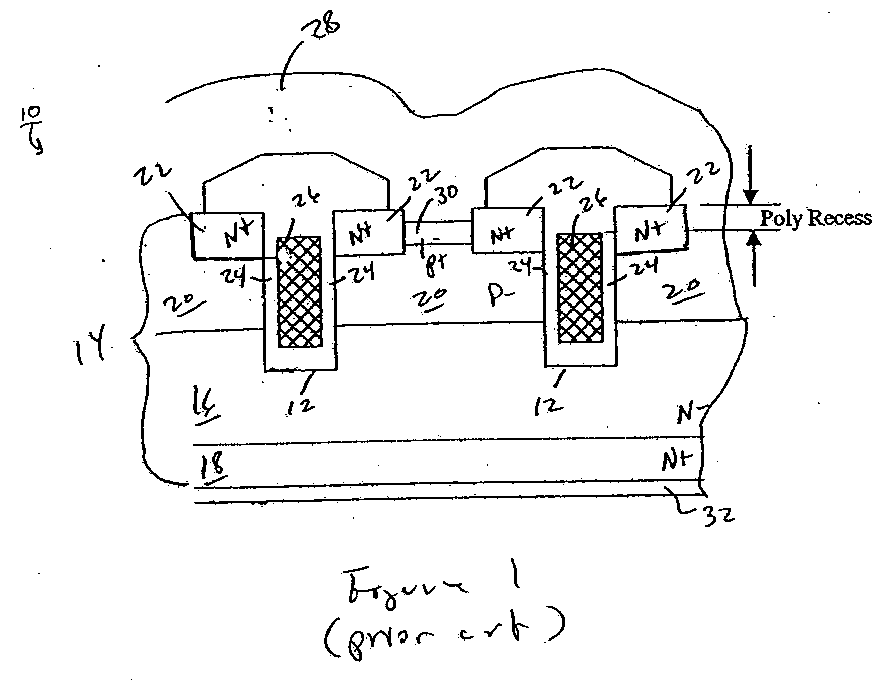
first embodiment
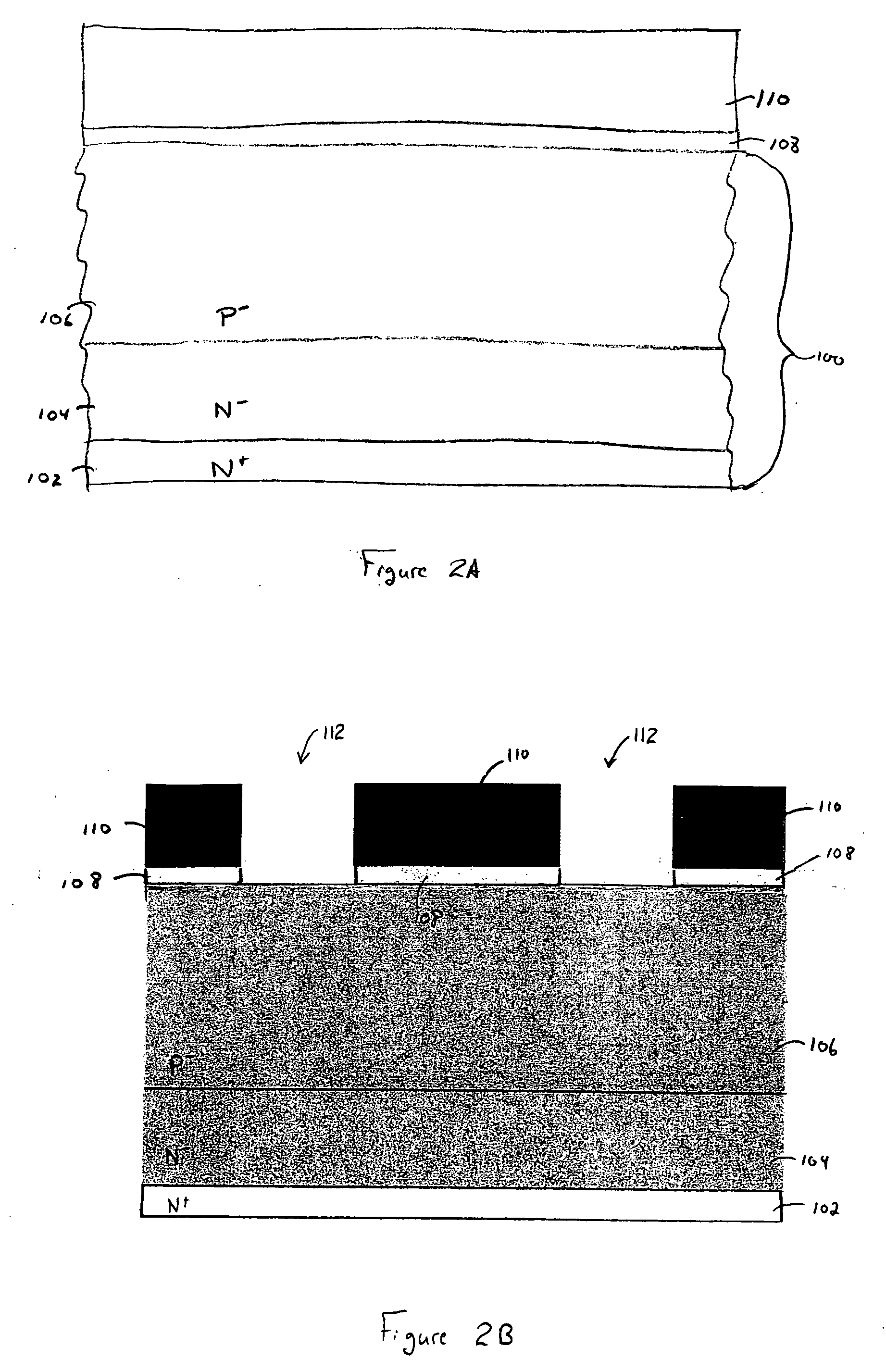
[0023] Referring to FIGS. 2A-2L (note that the Figures are not drawn to scale), a power MOSFET fabrication process according to the invention is illustrated, the fabrication process here resulting in gate electrodes that are recessed below the top surface of the semiconductor body. Beginning with FIG. 2A, there is shown an initial silicon body 100. Silicon body 100 preferably includes a silicon substrate 102 of one conductivity (e.g., N-type) and epitaxial silicon layer 104 of the same conductivity (e.g., N-type) grown over one major surface of silicon substrate 102. As is known, epitaxial silicon layer 104 includes a lower concentration of dopants as compared to substrate 102. Silicon body 100 also includes channel region 106, which has conductivity opposite to that of epitaxial silicon layer 104 (e.g. P-type). Preferably, channel region 106 is formed by implanting dopants on the surface of silicon layer 104 and driving these dopants in a diffusion drive to a desired channel depth....
second embodiment
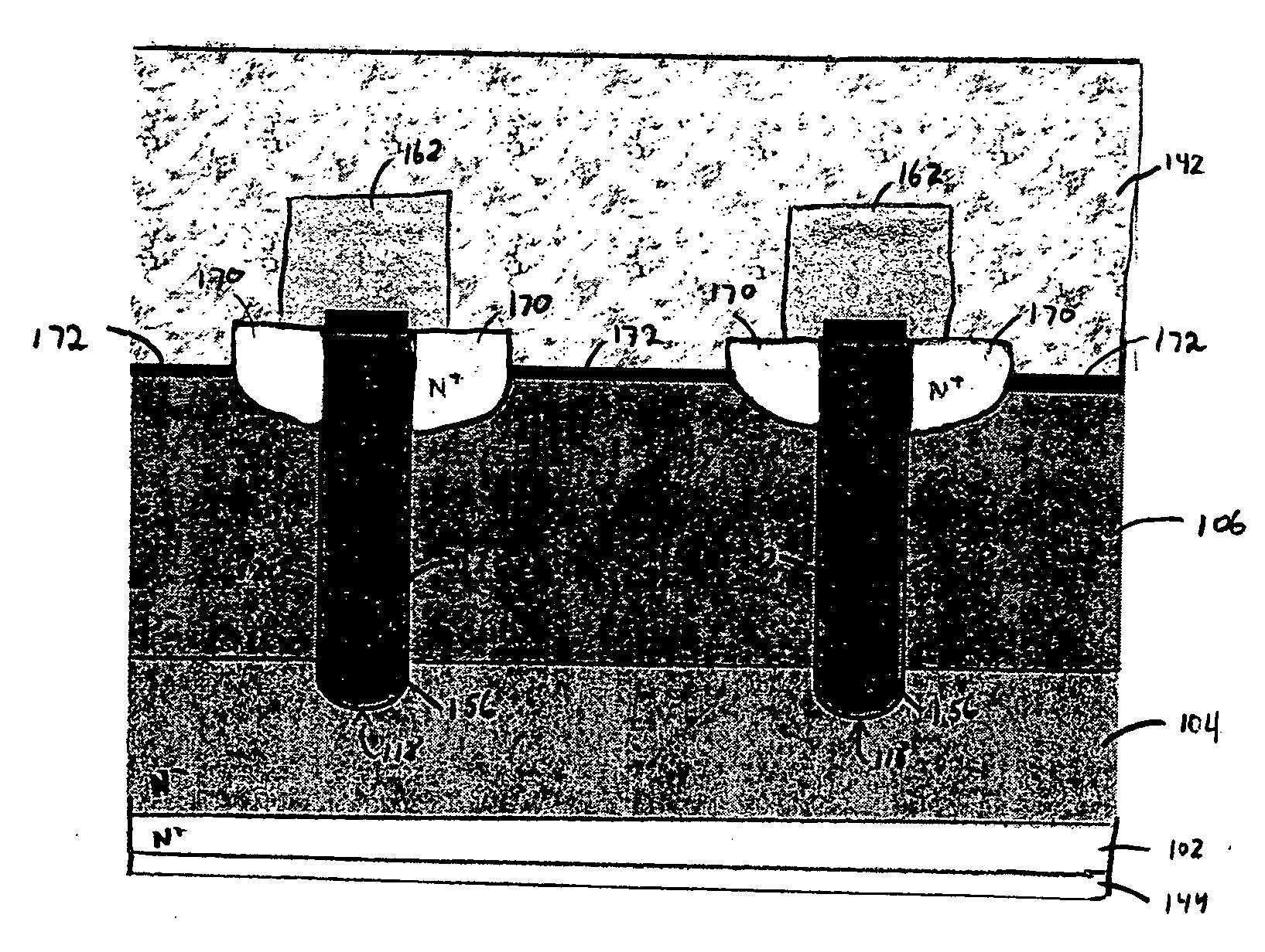
[0042] Referring to FIG. 4B, inside spacers 114 are next removed exposing a portion of channel region 108 along the upper edges of each trench 118. The process then proceeds similar to the second embodiment for the formation of the source regions. Specifically, a first source implant is next carried out to form source implant regions 160 in channel region 106 along the upper edges of each trench 118. However, again, a source diffusion drive is not carried out. Rather, a layer of oxide, composed from TEOS or the like for example, is formed over the surface of the structure, covering hard mask layer 110 and filling openings 112. This oxide layer is then etched back, forming insulation caps 162 over the gate electrodes 156. The resulting structure is shown in FIG. 4B.
[0043] Referring to FIG. 4C, an appropriate etching process is next carried out to remove the remaining hard mask layer 110 and pad oxide layer 108. As a result, openings 134 are formed between adjacent insulation caps 162...
PUM
 Abstract
Description
Claims
Application Information