Optical multi-gate device and method

a multi-gate device and optical technology, applied in the field of optical signal processing and switching, can solve the problems of curbing the operation efficiency of the electronic device, deceleration of electrons, and reducing the electric curren

Inactive Publication Date: 2005-09-29
DMITRY PONOMARENKO
View PDF9 Cites 12 Cited by
  • Summary
  • Abstract
  • Description
  • Claims
  • Application Information

AI Technical Summary

Benefits of technology

[0006] It is an object of the present invention to provide a system and a method for performing logical functions with optical light waves

Problems solved by technology

A prolonged response time curbs the operational efficiency of the electronic device.
The conduction of electric current through electronic devices, such as conductors, transistors, resistors, coils and capacitors, encounters inevitable retarding forces that decelerate the electrons and diminish the electric current.
These forces lead to the heating of the electronic device (with impractical exceptions such as ‘super-conductors’).
The intrinsic heating of transistors, which are condensed by millions

Method used


Image

  • Optical multi-gate device and method
  • Optical multi-gate device and method
  • Optical multi-gate device and method

Examples


Embodiment Construction

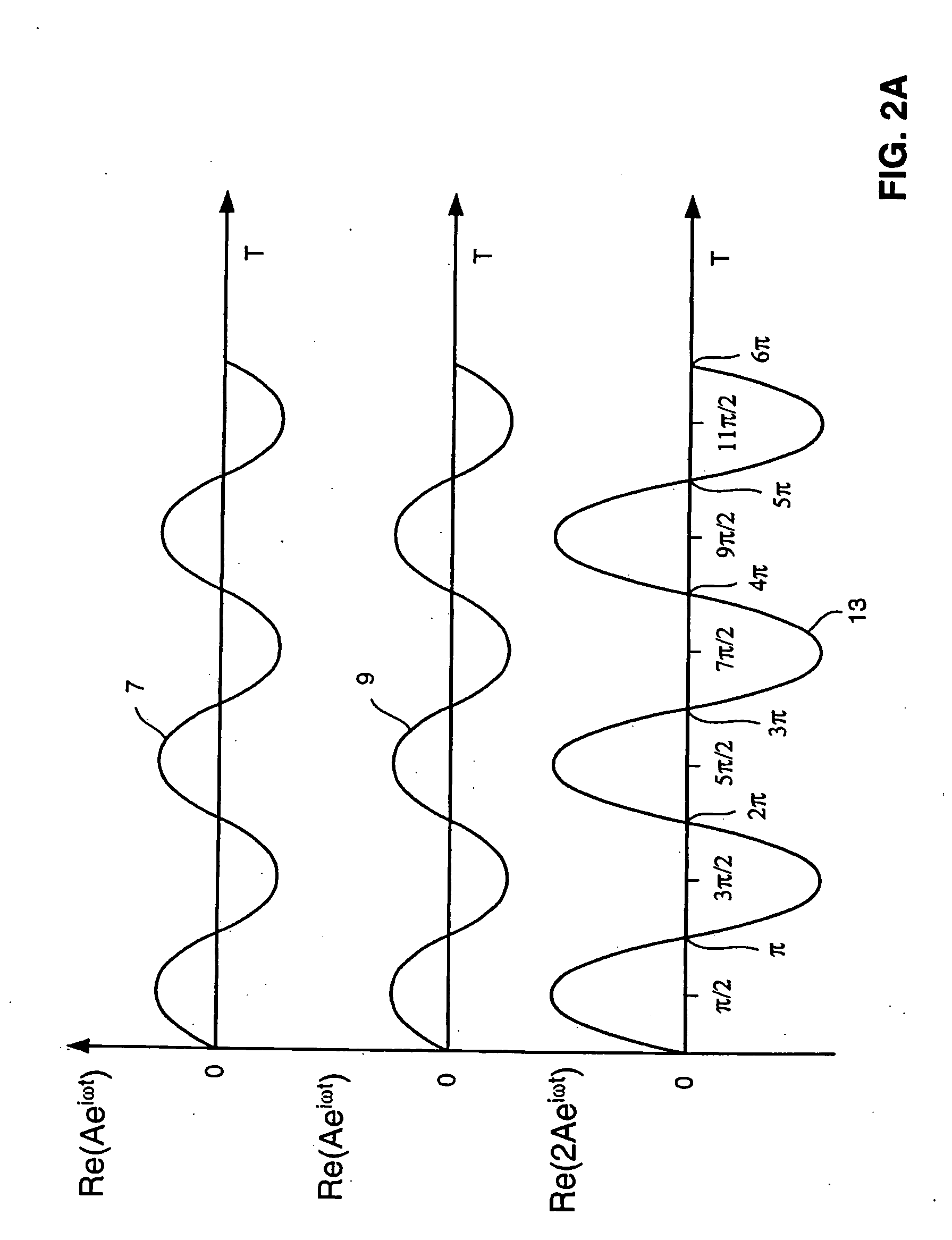
[0033] The present invention provides a system and a method for performing logical functions by employing optical light waves, thereby eliminating the use of electrical currents for operating such logical functions. A logical function is performed by superposing two incoming light beams at an optical junction, thereby producing an outgoing light beam. The phases and amplitudes of the incoming light beams define the characteristics of the outgoing light beam. A predetermined logical value—which is a function of the characteristics of the outgoing light beam, is determined when the outgoing light beam is detected.

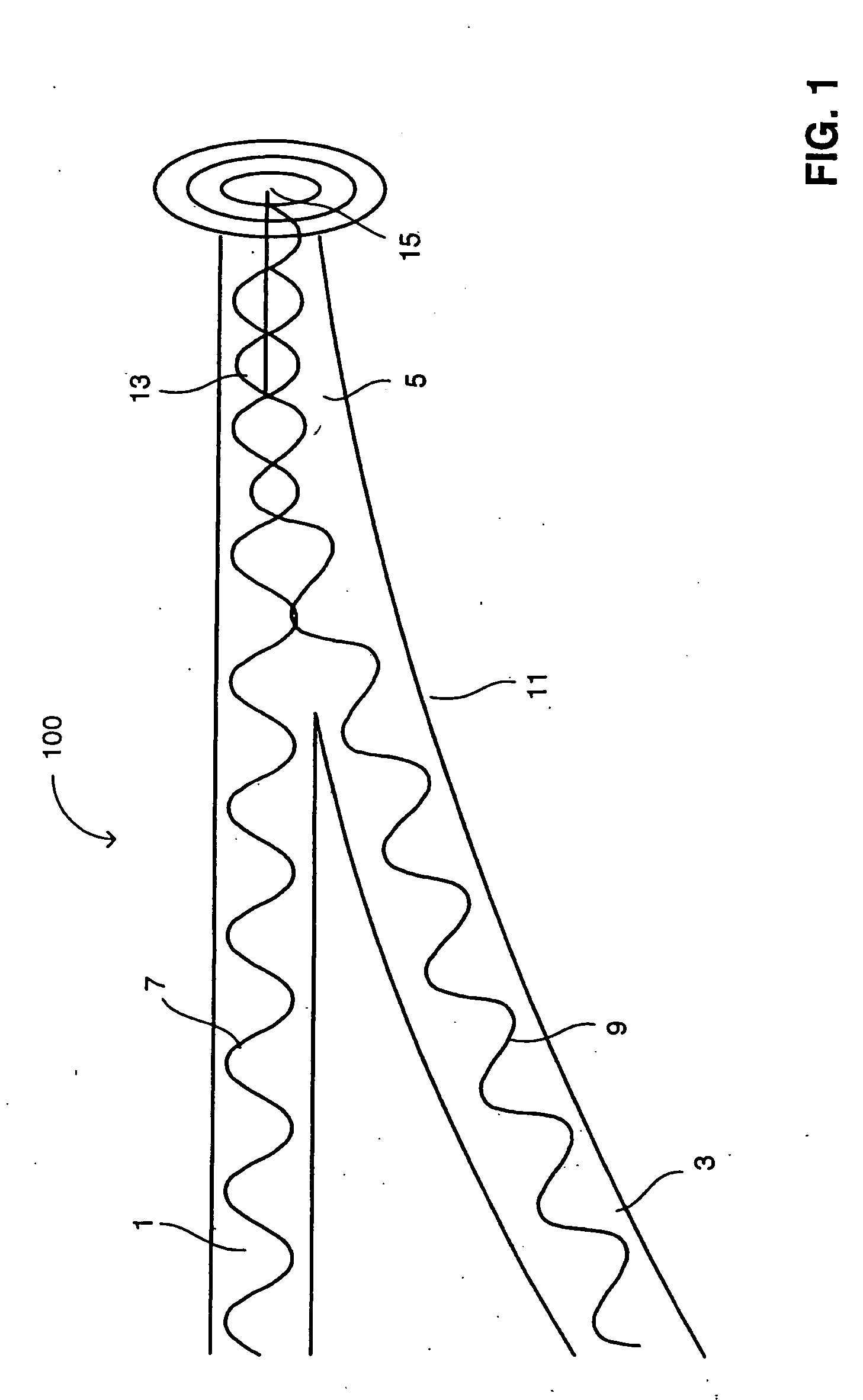
[0034] Reference is now made to FIG. 1, which is a schematic illustration of an optical device, generally referenced 100, constructed and operative in accordance with a preferred embodiment of the present invention. Device 100 includes an inlet 1, an inlet 3 and an outlet 5, all of which are capable of guiding waves there through. Inlets 1 and 3 and outlet 5 are coupled toge...


PUM


Abstract

A logical element including an optical junction coupled to at least two optical inlets and to at least one optical outlet. Incoming light beams of coherent monochromatic light beams and the same uniform frequency are applied to the optical inlets, and their super-positioning is provided as an outgoing light beam(s) via the optical outlet to another logical element or to a light intensity gauge. The light intensity gauge measures light intensity in specific zone(s) of an interference pattern created by the outgoing light beam, dependent on phase shift difference between the components of the incoming light beams, and the measured intensity is correlated with intensity ranges predetermined to conjugate to logical integer values, such as Boolean or other integer numeric values. A multiplicity of logical elements can be installed to provide an optical processor. Parallel use of the same logical element is provided by the simultaneous application of sets of light beams. The sets do not interact with each other by means of differing characteristics, such as different frequencies, or polarizations of the sets. A corresponding method is also provided.

Description

FIELD OF THE INVENTION [0001] The present invention relates to optical signal processing and switching, and more particularly to multi-gate devices for processing optical energy in logical devices, switching, commutation and computing optical signals, light amplification, energy control, optical waveguides communication, data transmission and computer circuitry, including arithmetic and logic units. BACKGROUND OF THE INVENTION [0002] Contemporary technology prevalently involves electric currents for the operation of transistors and other electronic devices. The velocity of electric signals through conductors and semi-conductors, namely—the response time of the (semi)-conductor to the input of an electric signal, is bounded by the physical limits of electric currents. A prolonged response time curbs the operational efficiency of the electronic device. For example, the speed of electric current through a conducting medium is about 6,000 km / sec and through a semi-conductor, such as a P...

Claims


Application Information

Patent Timeline
IPC IPC(8): G02F1/21G02F3/00
CPCG02F3/00G02F1/21
Inventor PONOMARENKO, DMITRY
Owner DMITRY PONOMARENKO
Why Eureka
Try Eureka