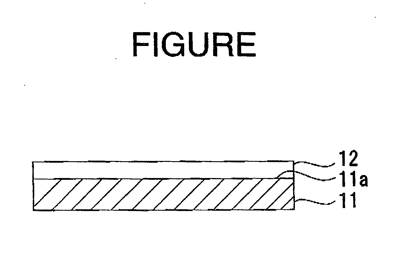
Radiation image storage panel
a technology of radiation image and storage panel, which is applied in the direction of conversion screens, instruments, nuclear engineering, etc., can solve the problems of defective points on the radiation image reproduced, abnormal phosphor crystal growth on the uneven area of the metal sheet, and disturb clinical examination and detection of the defective area of the examined object, etc., to achieve satisfactory graininess, less defective points, and high quality
- Summary
- Abstract
- Description
- Claims
- Application Information
AI Technical Summary
Benefits of technology
Problems solved by technology
Method used
Image
Examples
example 1
(1) Evaporation Source
[0053] As the evaporation sources, powdery cesium bromide (CsBr, purity: more than 4N) and powdery europium bromide (EuBr2, purity: more than 3N) were prepared. Each powder was once melted to remove water. For instance, the powdery EuBr2 was placed in a platinum crucible and heated to 800° C. in a tube furnace under halogen atmosphere. Each was analyzed according to ICP-MS method (Inductively Coupled Plasma Mass Spectrometry), to examine contents of impurities. As a result, the CsBr powder contained each of the alkali metals (Li, Na, K, Rb) other than Cs in an amount of 10 ppm or less and other elements such as alkaline earth metals (Mg, Ca, Sr, Ba) in amounts of 2 ppm or less. The EuBr2 powder contained each of the rare earth elements other than Eu in an amount of 20 ppm or less and other elements in amounts of 10 ppm or less. The evaporation sources were very hygroscopic, and hence were stored in a desiccator keeping a dry condition whose dew point was lowe...
example 2
[0057] The procedures of Example 1 were repeated except that the surface of the aluminum sheet was subjected to electrolytic polishing before the phosphor layer was deposited, to give a radiation image storage panel of the invention.
example 3
[0058] The procedures of Example 1 were repeated except that the surface of the aluminum sheet was plated with nickel before the phosphor layer was deposited, to give a radiation image storage panel of the invention.
PUM
| Property | Measurement | Unit |
|---|---|---|
| surface roughness Ra | aaaaa | aaaaa |
| surface roughness | aaaaa | aaaaa |
| surface roughness Rz | aaaaa | aaaaa |
Abstract
Description
Claims
Application Information
