Method and apparatus for reforming laminated films and laminated films manufactured thereby

a technology of laminated films and reforming processes, which is applied in the direction of electrical equipment, electric/magnetic/electromagnetic heating, electric discharge tubes, etc., can solve the problems of deterioration of the dielectric property of the interlayer insulating film, low mechanical strength of the sod film, and considerable deterioration of the dielectric property of the interlayer film, so as to increase the throughput of the reforming process, suppress the delamination

Inactive Publication Date: 2005-09-29
TOKYO ELECTRON LTD
View PDF2 Cites 17 Cited by
  • Summary
  • Abstract
  • Description
  • Claims
  • Application Information

AI Technical Summary

Benefits of technology

[0008] It is, therefore, an object of the present invention to provide a method for reforming laminated films, which is capable of increasing a throughput of a reforming process performed on the laminated films; preventing a deterioration of a low dielectric property; considerably suppressing a delamination by increasing an adhesivity between the laminated films; and improving a mechanical strength of interlayer insulating films, and the laminated films manufactured thereby.

Problems solved by technology

However, the SOD film is formed by coating a liquid material and some SOD films are formed to have a high porosity for a low dielectric constant and, therefore, the SOD film has a low mechanical strength.
Further, as in Reference 1, when each interlayer insulating film is composed of laminated films, each of the laminated films further requires the curing process using heat or electron beams, thereby deteriorating a throughput.
Moreover, since the interlayer insulating films are distributed over multiple layers, a thermal accumulation is getting bigger in an interlayer insulating film positioned at a lower layer and, further, the low dielectric property of the interlayer insulating film considerably deteriorates due to the heat applied in the curing process.
Accordingly, a desired low dielectric property cannot be obtained.
Besides, an interlayer insulating film formed by the spin coating method has a low mechanical strength.

Method used


Image

  • Method and apparatus for reforming laminated films and laminated films manufactured thereby
  • Method and apparatus for reforming laminated films and laminated films manufactured thereby
  • Method and apparatus for reforming laminated films and laminated films manufactured thereby

Examples


Embodiment Construction

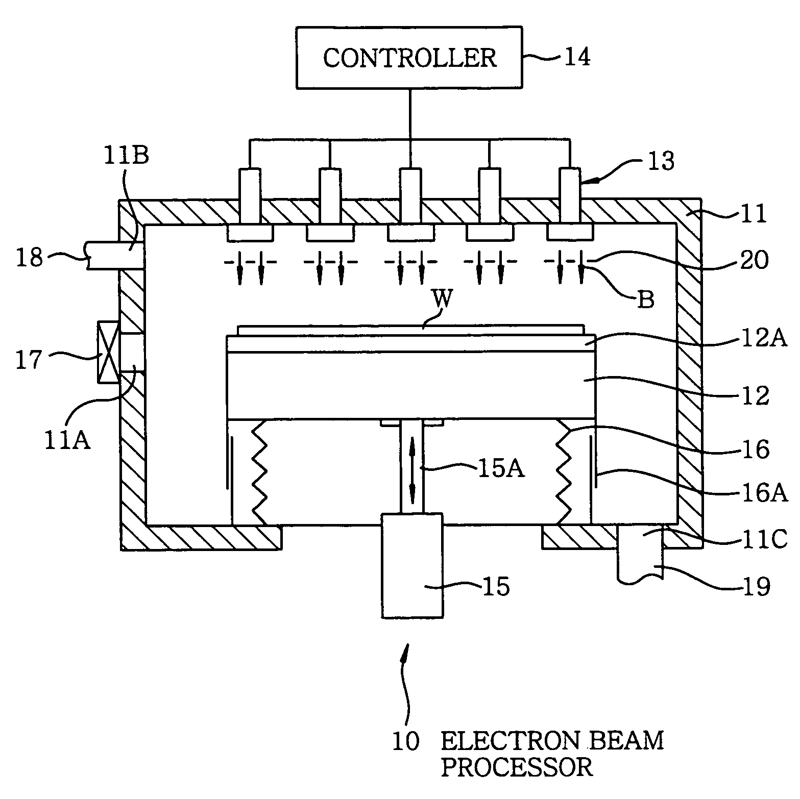
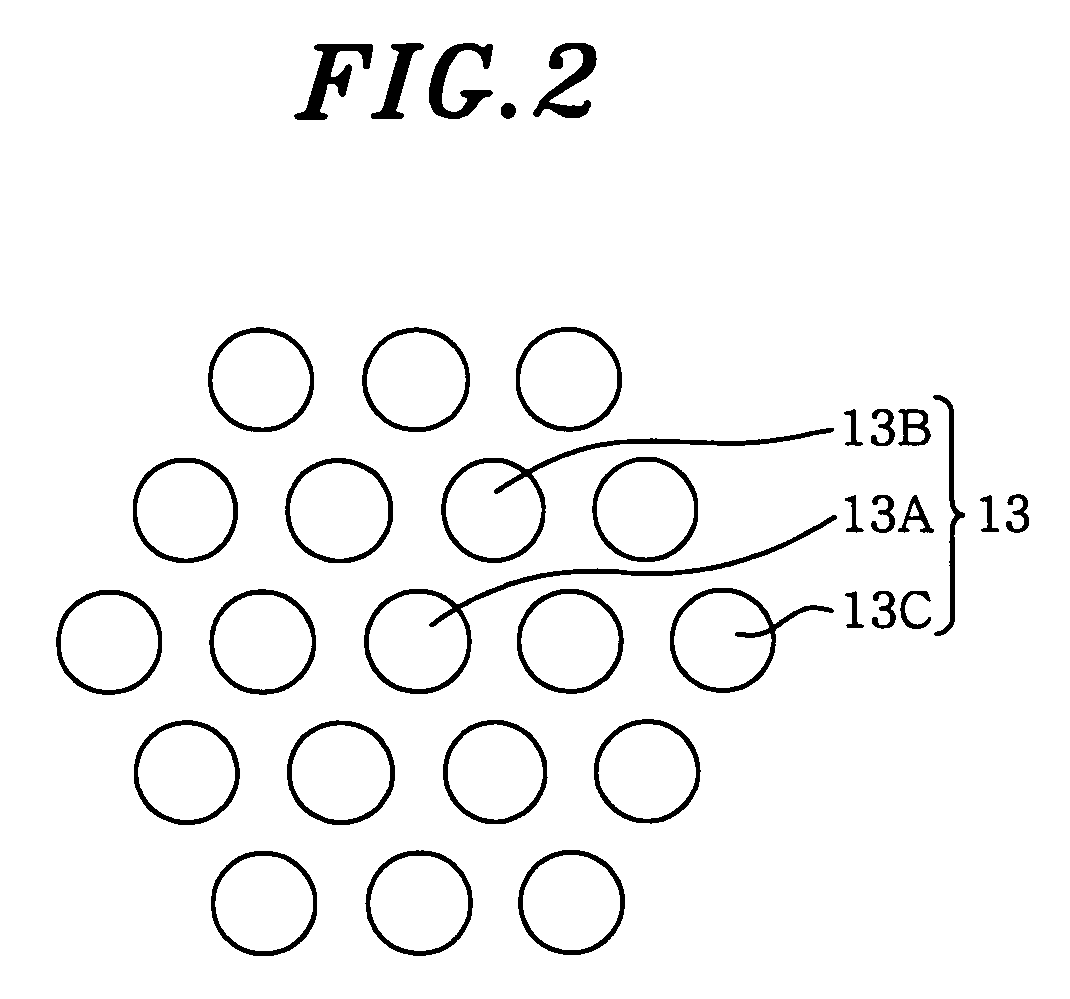
[0024] Hereinafter, the present invention will be described based on preferred embodiments illustrated in FIGS. 1 to 5. A laminated film manufacturing method of the present invention employs an electron beam processor shown in FIGS. 1 and 2. By using the electron beam processor, all of laminated films can be simultaneously reformed, thereby considerably increasing a throughput of a reforming process and improving adhesivity between the laminated films. Moreover, the laminated films include a porous lower film for realizing a low dielectric property; and a high density upper film (hard mask) for securing a mechanical strength, wherein the mechanical strength thereof is strengthened by employing an electron beam processing. Hereinafter, the electron beam processor used in this embodiment and the laminated films of this embodiment will be sequentially described.

[0025] As illustrated in FIG. 1, an electron beam processor 10 used in this embodiment includes, e.g., a depressurizable proc...


PUM

PropertyMeasurementUnit
elastic modulusaaaaaaaaaa

Abstract

There is provided a method for reforming laminated films, which simultaneously reforms a plurality of laminated films by irradiating electron beams on the laminated films. The method for reforming laminated films includes the steps of forming a lower film by coating a first low dielectric material in liquid form on a surface of a substrate; forming an upper film by coating a second low dielectric material in liquid form on the lower film; and irradiating electron beams on the lower and upper film. A laminated film manufacturing system includes a mounting table for mounting thereon a substrate on which the laminated films are formed; and an electron beam unit having a plurality of electron beam tubes for irradiating electron beams on the laminated films to thereby simultaneously reform the films.

Description

FIELD OF THE INVENTION [0001] The present invention relates to a method for reforming laminated films and laminated films manufactured thereby; and, more particularly, to a method for reforming laminated films capable of increasing a throughput of a reforming process performed on laminated films while increasing a mechanical strength and an adhesive strength between films and laminated films manufactured thereby. BACKGROUND OF THE INVENTION [0002] A wiring structure tends to become more complicated and a reduction of a parasitic capacitance caused by insulating films between wirings gets more important as the relentless drive toward high integration and high speed of semiconductor devices gets ever stronger. Accordingly, recently, in order to reduce the parasitic capacitance caused by the insulating films between the wirings in the complicated wiring structure, various organic and inorganic materials of a low dielectric constant have been developed, wherein such organic materials ar...

Claims


Application Information

Patent Timeline
Patent Type & Authority Applications(United States)
IPC IPC(8): H01L21/768B29C55/00H01J37/30H01L21/312H01L21/316H05B6/00
CPCH01J2237/316H01L21/02137H01L21/022H01L21/02203H01L21/76835H01L21/02351H01L21/3122H01L21/31633H01L21/76825H01L21/02282
Inventor HONDA, MINORUNAGAI, HIROYUKI
Owner TOKYO ELECTRON LTD
Why Eureka
Try Eureka