Stack-integrated package of optical transceiver for single core full duplex fiber communications

Inactive Publication Date: 2005-09-29
INTEGRATED CRYSTAL TECH
View PDF7 Cites 30 Cited by
  • Summary
  • Abstract
  • Description
  • Claims
  • Application Information

AI Technical Summary

Benefits of technology

[0008] It is therefore an object of the invention to provide a stack-integrated optical transceiver, by using a stack-integration package structure of a light emitter and a photodetector for high speed, full duplex optical fiber communication, It is another object of the invention to provide a stack-integrated

Problems solved by technology

These prior arts preclude collocation of the emitter and the photo-detector chips and require sophisti

Method used


Image

  • Stack-integrated package of optical transceiver for single core full duplex fiber communications
  • Stack-integrated package of optical transceiver for single core full duplex fiber communications
  • Stack-integrated package of optical transceiver for single core full duplex fiber communications

Examples


Example

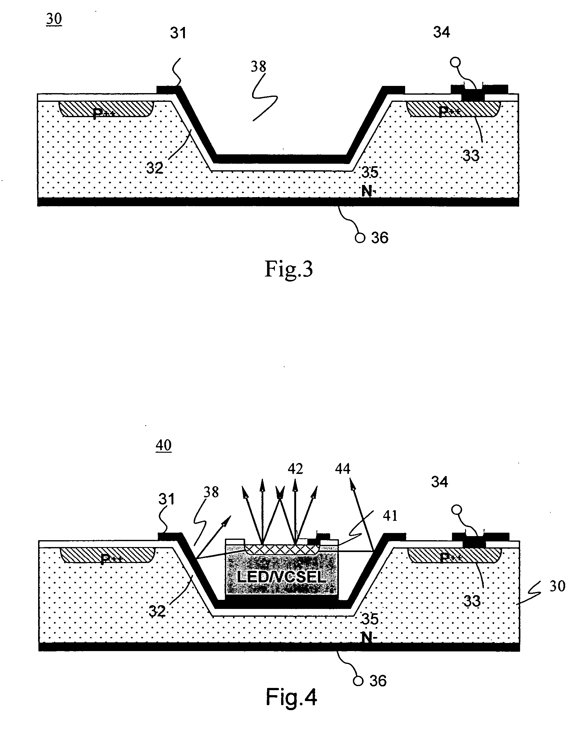
[0023] Referring to FIG. 3, a photodetector chip, or more specifically, a silicon photodiode 30, has a U-shaped cavity 38 that is surrounded by the optically active region, namely, the p-n junction area 33 of the photodiode 30. The cavity 38 can be formed using physical or chemical deep etching in semiconductor fabrication process deep to the substrate 35. After etching and cleaning, the surface of the cavity is coated by standard thermal oxidation 32 or other processes with an electrically insulating passivation first, then followed by a metal layer deposition on top. The metal layer is lithographically etched to a desired pattern, whereby the surface of the cavity is fully covered by cavity metal 31 so that it is reflective and opaque to light. This cavity metal layer 31 may also be connected to a bonding pad 34 on the upper surface of the photodetector for external wiring. A backside electrode 36 is deposited on the substrate 35.

[0024] As shown in FIG. 4, a light emitter chip 41...


PUM


Abstract

This invention relates to a novel stack-integration package of a light emitter and a photodetector in a high speed, full duplex optical transceiver for fiber communications. The structure is comprised of a photodetector chip, having an isolated micromachined cavity on the chip surface, and a light emitter chip, stacked on the bottom surface inside that cavity, so that a stack-integrated embodiment of light detector and emitter capable of performing full duplex optical communication is resulted. Said cavity surface in the photodetector is coated with reflective metal to prevent direct optical crosstalk from the emitter to the photodetector. Said light emitter means either LED (light emitting diode) or LD (laser diode). The present invention is further characterized by having a transparent encapsulation over the stack-integrated embodiment with a specific surface contour that minimizes the Fresnel reflection at the encapsulation-air interface and its associated crosstalk aftereffect. Such packaging structure is particularly suitable as a component for the purpose of single-core, full-duplex optical fiber communications.

Description

BACKGROUND OF THE INVENTION [0001] 1. Field of the Invention [0002] The present invention relates to a single-core full-duplex transceiver structure. In particular, the present invention relates to a novel stack-integration package of a light emitter and a photodetector in a high speed, full duplex optical transceiver for fiber communications. [0003] 2. Description of the Related Art [0004] Modern optical communications demand large quantity of high-speed photo-detectors and light emitting devices as the essential optical emitting and receiving components. In optical fiber communication links, a transmitter is the electrical to optical (E-O) converter, which is generally comprised of an LD (Laser Diode) or LED (Light Emitting Diode) and a driver IC as a package in a connector form while a receiver is an O-E converter comprising a PD (photodiode) and a signal processing IC packaged also in the same connector form for user friendly applications. [0005] An optical fiber that is fitted ...

Claims


Application Information

Patent Timeline
IPC IPC(8): H04B10/00H04B10/24
CPCH04B10/40
Inventor SHIE, JIN SHOWNHUANG, RONGNAN
Owner INTEGRATED CRYSTAL TECH
Why Eureka
Try Eureka